
Datasheet


PIC16F72X/PIC16LF72X
DS41341E-page 218 © 2009 Microchip Technology Inc.
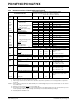
23.4 DC Characteristics: PIC16F72X/PIC16LF72X-I/E
DC CHARACTERISTICS
Standard Operating Conditions (unless otherwise stated)
Operating temperature -40°C ≤ TA ≤ +85°C for industrial
-40°C ≤ T
A ≤ +125°C for extended
Param
No.
Sym. Characteristic Min. Typ† Max. Units Conditions
V
IL Input Low Voltage
I/O PORT:
D030 with TTL buffer — — 0.8 V 4.5V ≤ V
DD ≤ 5.5V
D030A — — 0.15 V
DD V1.8V ≤ VDD ≤ 4.5V
D031 with Schmitt Trigger buffer — — 0.2 V
DD V2.0V ≤ VDD ≤ 5.5V
with I
2
C™ levels — — 0.3 VDD V
D032 MCLR
, OSC1 (RC mode)
(1)
——0.2VDD V
D033A OSC1 (HS mode) — — 0.3 V
DD V
V
IH Input High Voltage
I/O ports: — —
D040 with TTL buffer 2.0 — — V 4.5V ≤ V
DD ≤ 5.5V
D040A 0.25 V
DD +
0.8
——V1.8V ≤ VDD ≤ 4.5V
D041 with Schmitt Trigger buffer 0.8 V
DD ——V2.0V ≤ VDD ≤ 5.5V
with I
2
C™ levels 0.7 VDD ——V
D042 MCLR
0.8 VDD ——V
D043A OSC1 (HS mode) 0.7 V
DD ——V
D043B OSC1 (RC mode) 0.9 V
DD ——V(Note 1)
I
IL Input Leakage Current
(2)
D060 I/O ports — ± 5
± 5
± 125
± 1000
nA
nA
VSS ≤ VPIN ≤ VDD, Pin at high-
impedance, 85°C
125°C
D061 MCLR
(3)
—± 50± 200nAVSS ≤ VPIN ≤ VDD, 85°C
I
PUR PORTB Weak Pull-up Current
D070* 25
25
100
140
200
300 μA
V
DD = 3.3V, VPIN = VSS
VDD = 5.0V, VPIN = VSS
VOL Output Low Voltage
(4)
D080 I/O ports
——0.6V
IOL = 8mA, VDD = 5V
I
OL = 6mA, VDD = 3.3V
I
OL = 1.8mA, VDD = 1.8V
V
OH Output High Voltage
(4)
D090 I/O ports
V
DD - 0.7 — — V
I
OH = 3.5mA, VDD = 5V
I
OH = 3mA, VDD = 3.3V
I
OH = 1mA, VDD = 1.8V
Capacitive Loading Specs on Output Pins
D101* COSC2 OSC2 pin — — 15 pF In XT, HS and LP modes when
external clock is used to drive
OSC1
D101A* C
IO All I/O pins — — 50 pF
Legend: TBD = To Be Determined
* These parameters are characterized but not tested.
† Data in “Typ” column is at 3.0V, 25°C unless otherwise stated. These parameters are for design guidance only and are
not tested.
Note 1: In RC oscillator configuration, the OSC1/CLKIN pin is a Schmitt Trigger input. It is not recommended to use an external
clock in RC mode.
2: Negative current is defined as current sourced by the pin.
3: The leakage current on the MCLR
pin is strongly dependent on the applied voltage level. The specified levels represent
normal operating conditions. Higher leakage current may be measured at different input voltages.
4: Including OSC2 in CLKOUT mode.