
Datasheet


© 2009 Microchip Technology Inc. DS41341E-page 215
PIC16F72X/PIC16LF72X
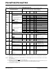
Supply Current (IDD)
(1, 2)
D014 — 290 330 μA1.8FOSC = 4 MHz
EC Oscillator mode
— 460 500 μA3.0
D014 — 300 430 μA 1.8 FOSC = 4 MHz
EC Oscillator mode (Note 5)
— 450 655 μA 3.0
— 500 730 μA 5.0
D015 — 100 130 μA1.8F
OSC = 500 kHz
MFINTOSC mode
— 120 150 μA3.0
D015 — 115 195 μA 1.8 FOSC = 500 kHz
MFINTOSC mode (Note 5)
— 135 200 μA 3.0
— 150 220 μA 5.0
D016 — 650 800 μA1.8F
OSC = 8 MHz
HFINTOSC mode
— 1000 1200 μA3.0
D016 — 625 850 μA 1.8 FOSC = 8 MHz
HFINTOSC mode (Note 5)
— 1000 1200 μA 3.0
— 1100 1500 μA 5.0
D017 — 1.0 1.2 mA 1.8 F
OSC = 16 MHz
HFINTOSC mode
— 1.5 1.85 mA 3.0
D017 — 1 1.2 mA 1.8 FOSC = 16 MHz
HFINTOSC mode (Note 5)
— 1.5 1.7 mA 3.0
— 1.7 2.1 mA 5.0
D018 — 210 240 μA1.8F
OSC = 4 MHz
EXTRC mode (Note 3, Note 5)
— 340 380 μA3.0
D018 — 225 320 μA 1.8 FOSC = 4 MHz
EXTRC mode (Note 3, Note 5)
— 360 445 μA 3.0
— 410 650 μA 5.0
D019 — 1.6 1.9 mA 3.0 F
OSC = 20 MHz
HS Oscillator mode
—2.02.8mA 3.6
D019 — 1.6 2 mA 3.0 FOSC = 20 MHz
HS Oscillator mode (Note 5)
— 1.9 3.2 mA 5.0
23.2 DC Characteristics: PIC16F72X/PIC16LF72X-I/E (Industrial, Extended) (Continued)
PIC16LF72X
Standard Operating Conditions (unless otherwise stated)
Operating temperature -40°C ≤ TA ≤ +85°C for industrial
-40°C ≤ T
A ≤ +125°C for extended
PIC16F72X
Standard Operating Conditions (unless otherwise stated)
Operating temperature -40°C ≤ T
A ≤ +85°C for industrial
-40°C ≤ T
A ≤ +125°C for extended
Param
No.
Device
Characteristics
Min. Typ† Max. Units
Conditions
V
DD Note
Note 1: The test conditions for all I
DD measurements in active operation mode are: OSC1 = external square wave, from
rail-to-rail; all I/O pins tri-stated, pulled to V
DD; MCLR = VDD; WDT disabled.
2: The supply current is mainly a function of the operating voltage and frequency. Other factors, such as I/O pin loading
and switching rate, oscillator type, internal code execution pattern and temperature, also have an impact on the current
consumption.
3: For RC oscillator configurations, current through R
EXT is not included. The current through the resistor can be extended
by the formula I
R = VDD/2REXT (mA) with REXT in kΩ.
4: FVR and BOR are disabled.
5: 0.1 μF capacitor on V
CAP (RA0).