
Datasheet


© 2009 Microchip Technology Inc. 41341E-page 133
PIC16F72X/PIC16LF72X
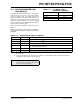
REGISTER 14-1: CPSCON0: CAPACITIVE SENSING CONTROL REGISTER 0
R/W-0 U-0 U-0 U-0 R/W-0 R/W-0 R-0 R/W-0
CPSON — — — CPSRNG1 CPSRNG0 CPSOUT T0XCS
bit 7 bit 0
Legend:
R = Readable bit W = Writable bit U = Unimplemented bit, read as ‘0’
-n = Value at POR ‘1’ = Bit is set ‘0’ = Bit is cleared x = Bit is unknown
bit 7 CPSON: Capacitive Sensing Module Enable bit
1 = Capacitive sensing module is operating
0 = Capacitive sensing module is shut off and consumes no operating current
bit 6-4 Unimplemented: Read as ‘0’
bit 3-2 CPSRNG<1:0>: Capacitive Sensing Oscillator Range bits
00 = Oscillator is off.
01 = Oscillator is in low range. Charge/discharge current is nominally 0.1 µA.
10 = Oscillator is in medium range. Charge/discharge current is nominally 1.2 µA.
11 = Oscillator is in high range. Charge/discharge current is nominally 18 µA.
bit 1 CPSOUT: Capacitive Sensing Oscillator Status bit
1 = Oscillator is sourcing current (Current flowing out the pin)
0 = Oscillator is sinking current (Current flowing into the pin)
bit 0 T0XCS: Timer0 External Clock Source Select bit
If T0CS =
1
The T0XCS bit controls which clock external to the core/Timer0 module supplies Timer0:
1 = Timer0 Clock Source is the capacitive sensing oscillator
0 = Timer0 Clock Source is the T0CKI pin
If T0CS =
0
Timer0 clock source is controlled by the core/Timer0 module and is FOSC/4.