
Datasheet


2010-2012 Microchip Technology Inc. DS41417B-page 101
PIC16(L)F722A/723A
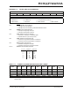
TABLE 11-1: SUMMARY OF REGISTERS ASSOCIATED WITH TIMER0
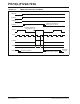
REGISTER 11-1: OPTION_REG: OPTION REGISTER
R/W-1 R/W-1 R/W-1 R/W-1 R/W-1 R/W-1 R/W-1 R/W-1
RBPU INTEDG T0CS T0SE PSA PS2 PS1 PS0
bit 7 bit 0
Legend:
R = Readable bit W = Writable bit U = Unimplemented bit, read as ‘0’
-n = Value at POR ‘1’ = Bit is set ‘0’ = Bit is cleared x = Bit is unknown
bit 7 RBPU
: PORTB Pull-up Enable bit
1 = PORTB pull-ups are disabled
0 = PORTB pull-ups are enabled by individual PORT latch values
bit 6 INTEDG: Interrupt Edge Select bit
1 = Interrupt on rising edge of INT pin
0 = Interrupt on falling edge of INT pin
bit 5 T0CS: TMR0 Clock Source Select bit
1 = Transition on T0CKI pin or CPSOSC signal
0 = Internal instruction cycle clock (FOSC/4)
bit 4 T0SE: TMR0 Source Edge Select bit
1 = Increment on high-to-low transition on T0CKI pin
0 = Increment on low-to-high transition on T0CKI pin
bit 3 PSA: Prescaler Assignment bit
1 = Prescaler is assigned to the WDT
0 = Prescaler is assigned to the Timer0 module
bit 2-0 PS<2:0>: Prescaler Rate Select bits
000
001
010
011
100
101
110
111
1 : 2
1 : 4
1 : 8
1 : 16
1 : 32
1 : 64
1 : 128
1 : 256
1 : 1
1 : 2
1 : 4
1 : 8
1 : 16
1 : 32
1 : 64
1 : 128
B
IT VALUE TMR0 RATE WDT RATE
Name Bit 7 Bit 6 Bit 5 Bit 4 Bit 3 Bit 2 Bit 1 Bit 0
Register on
Page
CPSCON0
CPSON — — — CPSRNG1 CPSRNG0 CPSOUT T0XCS 121
INTCON GIE PEIE T0IE INTE RBIE T0IF INTF RBIF 40
OPTION_REG
RBPU INTEDG T0CS T0SE PSA PS2 PS1 PS0 101
TMR0 Timer0 Module Register —
TRISA
TRISA7 TRISA6 TRISA5 TRISA4 TRISA3 TRISA2 TRISA1 TRISA0 48
Legend: – = Un implemented locations, read as ‘0’, u = unchanged, x = unknown. Shaded cells are not used by the
Timer0 module.