
Information


PIC16F72X/PIC16LF72X
DS41341E-page 232 © 2009 Microchip Technology Inc.
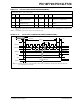
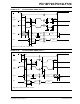
FIGURE 23-13: PIC16F72X A/D CONVERSION TIMING (SLEEP MODE)
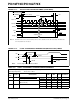
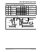
FIGURE 23-14: USART SYNCHRONOUS TRANSMISSION (MASTER/SLAVE) TIMING
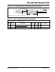
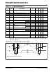
TABLE 23-9: USART SYNCHRONOUS TRANSMISSION REQUIREMENTS
AD132
AD131
AD130
BSF ADCON0, GO
Q4
A/D CLK
A/D Data
ADRES
ADIF
GO
Sample
OLD_DATA
Sampling Stopped
DONE
NEW_DATA
7 5 3210
Note 1: If the A/D clock source is selected as RC, a time of T
CY is added before the A/D clock starts. This allows the
SLEEP instruction to be executed.
AD134
4
6
1 TCY
(TOSC/2 + TCY
(1)
)
1 TCY
Standard Operating Conditions (unless otherwise stated)
Operating Temperature -40°C ≤ T
A ≤ +125°C
Param.
No.
Symbol Characteristic Min. Max. Units Conditions
US120 T
CKH2DTV SYNC XMIT (Master and Slave)
Clock high to data-out valid
3.0-5.5V — 80 ns
1.8-5.5V — 100 ns
US121 T
CKRF Clock out rise time and fall time
(Master mode)
3.0-5.5V — 45 ns
1.8-5.5V — 50 ns
US122 T
DTRF Data-out rise time and fall time 3.0-5.5V — 45 ns
1.8-5.5V — 50 ns
Note: Refer to Figure 23-2 for load conditions.
US121
US121
US120
US122
CK
DT