
Datasheet


Table Of Contents
- High-Performance RISC CPU:
- Special Microcontroller Features:
- Low-Power Features:
- Peripheral Features:
- PIC16F631 Pin Diagram
- PIC16F677 Pin Diagram
- PIC16F685 Pin Diagram
- PIC16F687/689 Pin Diagram
- PIC16F690 Pin Diagram (PDIP, SOIC, SSOP)
- PIC16F631/677/685/687/689/690 Pin Diagram (QFN)
- Most Current Data Sheet
- Errata
- Customer Notification System
- 1.0 Device Overview
- FIGURE 1-1: PIC16F631 Block Diagram
- FIGURE 1-2: PIC16F677 Block Diagram
- FIGURE 1-3: PIC16F685 Block Diagram
- FIGURE 1-4: PIC16F687/PIC16F689 Block Diagram
- FIGURE 1-5: PIC16F690 Block Diagram
- TABLE 1-1: Pinout Description - PIC16F631
- TABLE 1-2: Pinout Description - PIC16F677
- TABLE 1-3: Pinout Description - PIC16F685
- TABLE 1-4: Pinout Description - PIC16F687/PIC16F689
- TABLE 1-5: Pinout Description - PIC16F690
- 2.0 Memory Organization
- 2.1 Program Memory Organization
- 2.2 Data Memory Organization
- 2.2.1 General Purpose Register File
- 2.2.2 Special Function Registers
- FIGURE 2-4: PIC16F631 Special Function Registers
- FIGURE 2-5: PIC16F677 Special Function Registers
- FIGURE 2-6: PIC16F685 Special Function Registers
- FIGURE 2-7: PIC16F687/PIC16F689 Special Function Registers
- FIGURE 2-8: PIC16F690 Special Function Registers
- TABLE 2-1: PIC16F631/677/685/687/689/690 Special Function Registers Summary Bank 0
- TABLE 2-2: PIC16F631/677/685/687/689/690 Special Function Registers Summary Bank 1
- TABLE 2-3: PIC16F631/677/685/687/689/690 Special Function Registers Summary Bank 2
- TABLE 2-4: PIC16F631/677/685/687/689/690 Special Function Registers Summary Bank 3
- Register 2-1: STATUS: STATUS Register
- Register 2-2: OPTION_REG: Option Register
- Register 2-3: INTCON: Interrupt Control Register
- Register 2-4: PIE1: Peripheral Interrupt Enable Register 1
- Register 2-5: PIE2: Peripheral Interrupt Enable Register 2
- Register 2-6: PIR1: Peripheral Interrupt Request Register 1
- Register 2-7: PIR2: Peripheral Interrupt Request Register 2
- Register 2-8: PCON: Power Control Register
- 2.3 PCL and PCLATH
- 2.4 Indirect Addressing, INDF and FSR Registers
- 3.0 Oscillator Module (With Fail-Safe Clock Monitor)
- 4.0 I/O Ports
- 4.1 PORTA and the TRISA Registers
- 4.2 Additional Pin Functions
- 4.3 PORTB and TRISB Registers
- 4.4 Additional PORTB Pin Functions
- 4.5 PORTC and TRISC Registers
- 5.0 Timer0 Module
- 6.0 Timer1 Module with Gate Control
- 6.1 Timer1 Operation
- 6.2 Clock Source Selection
- 6.3 Timer1 Prescaler
- 6.4 Timer1 Oscillator
- 6.5 Timer1 Operation in Asynchronous Counter Mode
- 6.6 Timer1 Gate
- 6.7 Timer1 Interrupt
- 6.8 Timer1 Operation During Sleep
- 6.9 ECCP Capture/Compare Time Base
- 6.10 ECCP Special Event Trigger
- 6.11 Comparator Synchronization
- 6.12 Timer1 Control Register
- 7.0 Timer2 Module
- 8.0 Comparator Module
- 8.1 Comparator Overview
- 8.2 Comparator Control
- 8.3 Comparator Response Time
- 8.4 Comparator Interrupt Operation
- 8.5 Operation During Sleep
- 8.6 Effects of a Reset
- 8.7 Analog Input Connection Considerations
- 8.8 Additional Comparator Features
- 8.9 Comparator SR Latch
- 8.10 Comparator Voltage Reference
- 9.0 Analog-to-Digital Converter (ADC) Module
- FIGURE 9-1: ADC Block Diagram
- 9.1 ADC Configuration
- 9.2 ADC Operation
- 9.2.1 Starting A Conversion
- 9.2.2 Completion of a Conversion
- 9.2.3 Terminating a conversion
- 9.2.4 ADC Operation During Sleep
- 9.2.5 SPecial Event Trigger
- 9.2.6 A/D Conversion Procedure
- 9.2.7 ADC Register Definitions
- Register 9-1: ADCON0: A/D Control Register 0
- Register 9-2: ADCON1: A/D Control Register 1
- Register 9-3: ADRESH: ADC Result Register High (ADRESH) ADFM = 0
- Register 9-4: ADRESL: ADC Result Register Low (ADRESL) ADFM = 0
- Register 9-5: ADRESH: ADC Result Register High (ADRESH) ADFM = 1
- Register 9-6: ADRESL: ADC Result Register Low (ADRESL) ADFM = 1
- 9.3 A/D Acquisition Requirements
- 10.0 Data EEPROM and Flash Program Memory Control
- 10.1 EEADR and EEADRH Registers
- 10.2 Write Verify
- 10.3 Protection Against Spurious Write
- 10.4 Data EEPROM Operation During Code-Protect
- 11.0 Enhanced Capture/Compare/PWM Module
- TABLE 11-1: ECCP Mode - Timer Resources Required
- Register 11-1: CCP1CON: Enhanced CCP1 Control Register
- 11.1 Capture Mode
- 11.2 Compare Mode
- 11.3 PWM Mode
- 11.4 PWM (Enhanced Mode)
- FIGURE 11-5: Example Simplified Block Diagram of the Enhanced PWM Mode
- TABLE 11-4: example Pin Assignments for Various PWM Enhanced Modes
- FIGURE 11-6: Example PWM (enhanced Mode) Output Relationships (Active-High State)
- FIGURE 11-7: Example Enhanced PWM Output Relationships (Active-Low State)
- 11.4.1 Half-Bridge Mode
- 11.4.2 Full-Bridge Mode
- 11.4.3 Start-up Considerations
- 11.4.4 Enhanced PWM Auto-shutdown mode
- 11.4.5 Auto-Restart Mode
- 11.4.6 Programmable Dead-Band Delay mode
- 11.4.7 Pulse Steering Mode
- Register 11-4: PSTRCON: Pulse Steering Control Register(1)
- FIGURE 11-19: Simplified Steering Block Diagram
- FIGURE 11-20: Example of Steering Event at End of Instruction (STRSYNC = 0)
- FIGURE 11-21: Example of Steering Event at Beginning of Instruction (STRSYNC = 1)
- TABLE 11-5: Summary of Registers Associated with Capture, Compare and PWM
- 12.0 Enhanced Universal Synchronous Asynchronous Receiver Transmitter (EUSART)
- FIGURE 12-1: EUSART Transmit Block Diagram
- FIGURE 12-2: EUSART Receive Block Diagram
- 12.1 EUSART Asynchronous Mode
- 12.2 Clock Accuracy with Asynchronous Operation
- 12.3 EUSART Baud Rate Generator (BRG)
- 12.4 EUSART Synchronous Mode
- 12.5 EUSART Operation During Sleep
- 13.0 SSP Module Overview
- 13.1 SPI Mode
- 13.2 Operation
- 13.3 Enabling SPI I/O
- 13.4 Typical Connection
- 13.5 Master Mode
- 13.6 Slave Mode
- 13.7 Slave Select Synchronization
- 13.8 Sleep Operation
- 13.9 Effects of a Reset
- 13.10 Bus Mode Compatibility
- 13.11 SSP I2C Operation
- 13.12 Slave Mode
- 13.13 Master Mode
- 13.14 Multi-Master Mode
- 14.0 Special Features of the CPU
- 14.1 Configuration Bits
- 14.2 Reset
- FIGURE 14-1: Simplified Block Diagram of On-chip Reset Circuit
- 14.2.1 Power-on Reset (POR)
- 14.2.2 MCLR
- 14.2.3 Power-up Timer (PWRT)
- 14.2.4 Brown-out Reset (BOR)
- 14.2.5 Time-out Sequence
- 14.2.6 Power Control (PCON) Register
- TABLE 14-1: Time-out in Various Situations
- TABLE 14-2: Status/PCON Bits and Their Significance
- TABLE 14-3: Summary of Registers Associated with Brown-out
- FIGURE 14-4: Time-out Sequence On Power-up (Delayed MCLR): Case 1
- FIGURE 14-5: Time-out Sequence On Power-up (Delayed MCLR): Case 2
- FIGURE 14-6: Time-out Sequence on Power-up (MCLR with Vdd)
- TABLE 14-4: Initialization Condition for Register
- TABLE 14-5: Initialization Condition for Special Registers
- 14.3 Interrupts
- 14.4 Context Saving During Interrupts
- 14.5 Watchdog Timer (WDT)
- 14.6 Power-Down Mode (Sleep)
- 14.7 Code Protection
- 14.8 ID Locations
- 14.9 In-Circuit Serial Programming
- 15.0 Instruction Set Summary
- 16.0 Development Support
- 16.1 MPLAB Integrated Development Environment Software
- 16.2 MPASM Assembler
- 16.3 MPLAB C18 and MPLAB C30 C Compilers
- 16.4 MPLINK Object Linker/ MPLIB Object Librarian
- 16.5 MPLAB ASM30 Assembler, Linker and Librarian
- 16.6 MPLAB SIM Software Simulator
- 16.7 MPLAB ICE 2000 High-Performance In-Circuit Emulator
- 16.8 MPLAB REAL ICE In-Circuit Emulator System
- 16.9 MPLAB ICD 2 In-Circuit Debugger
- 16.10 MPLAB PM3 Device Programmer
- 16.11 PICSTART Plus Development Programmer
- 16.12 PICkit 2 Development Programmer
- 16.13 Demonstration, Development and Evaluation Boards
- 17.0 Electrical Specifications
- Absolute Maximum Ratings(†)
- 17.1 DC Characteristics: PIC16F631/677/685/687/689/690-I (Industrial) PIC16F631/677/685/687/689/690-E (Extended)
- 17.2 DC Characteristics: PIC16F631/677/685/687/689/690-I (Industrial) PIC16F631/677/685/687/689/690-E (Extended)
- 17.3 DC Characteristics: PIC16F631/677/685/687/689/690-E (Extended)
- 17.4 DC Characteristics: PIC16F631/677/685/687/689/690-I (Industrial) PIC16F631/677/685/687/689/690-E (Extended)
- 17.5 Thermal Considerations
- 17.6 Timing Parameter Symbology
- 17.7 AC Characteristics: PIC16F631/677/685/687/689/690 (Industrial, Extended)
- FIGURE 17-4: Clock Timing
- TABLE 17-1: Clock Oscillator Timing Requirements
- TABLE 17-2: Oscillator Parameters
- FIGURE 17-5: CLKOUT and I/O Timing
- TABLE 17-3: CLKOUT and I/O Timing Parameters
- FIGURE 17-6: Reset, Watchdog Timer, Oscillator Start-up Timer and Power-up Timer Timing
- FIGURE 17-7: Brown-out Reset Timing and Characteristics
- TABLE 17-4: Reset, Watchdog Timer, Oscillator Start-up Timer, Power-up Timer and Brown-out Reset Parameters
- FIGURE 17-8: Timer0 and Timer1 External Clock Timings
- TABLE 17-5: Timer0 and Timer1 External Clock Requirements
- FIGURE 17-9: Capture/Compare/PWM Timings (ECCP)
- TABLE 17-6: Capture/Compare/PWM Requirements (ECCP)
- TABLE 17-7: Comparator Specifications
- TABLE 17-8: Comparator Voltage Reference (CVref) Specifications
- TABLE 17-9: Voltage (VR) Reference Specifications
- FIGURE 17-10: EUSART Synchronous Transmission (Master/Slave) Timing
- TABLE 17-10: EUSART Synchronous Transmission Requirements
- FIGURE 17-11: EUSART Synchronous Receive (Master/Slave) Timing
- TABLE 17-11: EUSART Synchronous Receive Requirements
- FIGURE 17-12: SPI Master Mode Timing (CKE = 0, SMP = 0)
- FIGURE 17-13: SPI Master Mode Timing (CKE = 1, SMP = 1)
- FIGURE 17-14: SPI Slave Mode Timing (CKE = 0)
- FIGURE 17-15: SPI Slave Mode Timing (CKE = 1)
- TABLE 17-12: SPI Mode requirements
- FIGURE 17-16: I2C™ Bus Start/Stop Bits Timing
- TABLE 17-13: I2C™ Bus Start/Stop Bits Requirements
- FIGURE 17-17: I2C™ Bus Data Timing
- TABLE 17-14: I2C™ Bus Data Requirements
- TABLE 17-15: A/D Converter (ADC) Characteristics:
- FIGURE 17-18: A/D Conversion Timing (Normal Mode)
- TABLE 17-16: A/D Conversion Requirements
- FIGURE 17-19: A/D Conversion Timing (Sleep Mode)
- 18.0 DC and AC Characteristics Graphs and Tables
- FIGURE 18-1: Typical Idd vs. Fosc Over Vdd (EC Mode)
- FIGURE 18-2: Maximum Idd vs. Fosc Over Vdd (EC Mode)
- FIGURE 18-3: Typical Idd vs. Fosc Over Vdd (HS Mode)
- FIGURE 18-4: Maximum Idd vs. Fosc Over Vdd (HS Mode)
- FIGURE 18-5: Typical Idd vs. Vdd Over Fosc (XT Mode)
- FIGURE 18-6: Maximum Idd vs. Vdd Over Fosc (XT Mode)
- FIGURE 18-7: Idd vs. Vdd (LP Mode)
- FIGURE 18-8: Typical Idd vs. Vdd Over Fosc (EXTRC Mode)
- FIGURE 18-9: Maximum Idd vs. Vdd Over Fosc (EXTRC Mode)
- FIGURE 18-10: Idd vs. Vdd Over Fosc (LFINTOSC Mode, 31 kHz)
- FIGURE 18-11: Typical Idd vs. Fosc Over Vdd (HFINTOSC Mode)
- FIGURE 18-12: Maximum Idd vs. Fosc Over Vdd (HFINTOSC Mode)
- FIGURE 18-13: Typical Ipd vs. Vdd (Sleep Mode, all Peripherals Disabled)
- FIGURE 18-14: Maximum Ipd vs. Vdd (Sleep Mode, all Peripherals Disabled)
- FIGURE 18-15: Comparator Ipd vs. Vdd (Both Comparators Enabled)
- FIGURE 18-16: BOR Ipd VS. Vdd Over Temperature
- FIGURE 18-17: Typical WDT Ipd VS. Vdd Over Temperature
- FIGURE 18-18: Maximum WDT Ipd VS. Vdd Over Temperature
- FIGURE 18-19: WDT Period VS. Vdd Over Temperature
- FIGURE 18-20: WDT Period VS. Temperature Over Vdd (5.0V)
- FIGURE 18-21: CVref Ipd VS. Vdd Over Temperature (High Range)
- FIGURE 18-22: CVref Ipd VS. Vdd Over Temperature (Low Range)
- FIGURE 18-23: Typical VP6 Reference Ipd vs. Vdd (25 C)
- FIGURE 18-24: Maximum VP6 Reference Ipd vs. Vdd Over Temperature
- FIGURE 18-25: T1OSC Ipd vs. Vdd Over Temperature (32 kHz)
- FIGURE 18-26: Vol VS. Iol Over Temperature (Vdd = 3.0V)
- FIGURE 18-27: Vol VS. Iol Over Temperature (Vdd = 5.0V)
- FIGURE 18-28: Voh VS. Ioh Over Temperature (Vdd = 3.0V)
- FIGURE 18-29: Voh VS. Ioh Over Temperature (Vdd = 5.0V)
- FIGURE 18-30: TTL Input Threshold Vin VS. Vdd Over Temperature
- FIGURE 18-31: Schmitt Trigger Input Threshold Vin VS. Vdd Over Temperature
- FIGURE 18-32: Comparator Response Time (Rising Edge)
- FIGURE 18-33: Comparator Response Time (Falling Edge)
- FIGURE 18-34: LFINTOSC Frequency vs. Vdd Over Temperature (31 kHz)
- FIGURE 18-35: ADC Clock Period vs. Vdd Over Temperature
- FIGURE 18-36: Typical HFINTOSC Start-Up Times vs. Vdd Over Temperature
- FIGURE 18-37: Maximum HFINTOSC Start-Up Times vs. Vdd Over Temperature
- FIGURE 18-38: Minimum HFINTOSC Start-Up Times vs. Vdd Over Temperature
- FIGURE 18-39: Typical HFINTOSC Frequency Change vs. Vdd (25 C)
- FIGURE 18-40: Typical HFINTOSC Frequency Change Over Device Vdd (85 C)
- FIGURE 18-41: Typical HFINTOSC Frequency Change vs. Vdd (125 C)
- FIGURE 18-42: Typical HFINTOSC Frequency Change vs. Vdd (-40 C)
- FIGURE 18-43: Typical VP6 Reference Voltage vs. Vdd (25 C)
- FIGURE 18-44: Typical VP6 Reference Voltage Over Temperature (3V)
- FIGURE 18-45: Typical VP6 Reference Voltage Over Temperature (5V)
- FIGURE 18-46: Typical VP6 Reference Voltage Distribution (3V, 25 C)
- FIGURE 18-47: Typical VP6 Reference Voltage Distribution (3V, 85 C)
- FIGURE 18-48: Typical VP6 Reference Voltage Distribution (3V, 125 C)
- FIGURE 18-49: Typical VP6 Reference Voltage Distribution (3V, -40 C)
- FIGURE 18-50: Typical VP6 Reference Voltage Distribution (5V, 25 C)
- FIGURE 18-51: Typical VP6 Reference Voltage Distribution (5V, 85 C)
- FIGURE 18-52: Typical VP6 Reference Voltage Distribution (5V, 125 C)
- FIGURE 18-53: Typical VP6 Reference Voltage Distribution (5V, -40 C)
- 19.0 Packaging Information
- Appendix A: Data Sheet Revision History
- Appendix B: Migrating from other PIC® Devices
- INDEX
- The Microchip Web Site
- Customer Change Notification Service
- Customer Support
- Reader Response
- Product Identification System
- Worldwide Sales
PIC16F631/677/685/687/689/690
DS41262E-page 248 © 2008 Microchip Technology Inc.
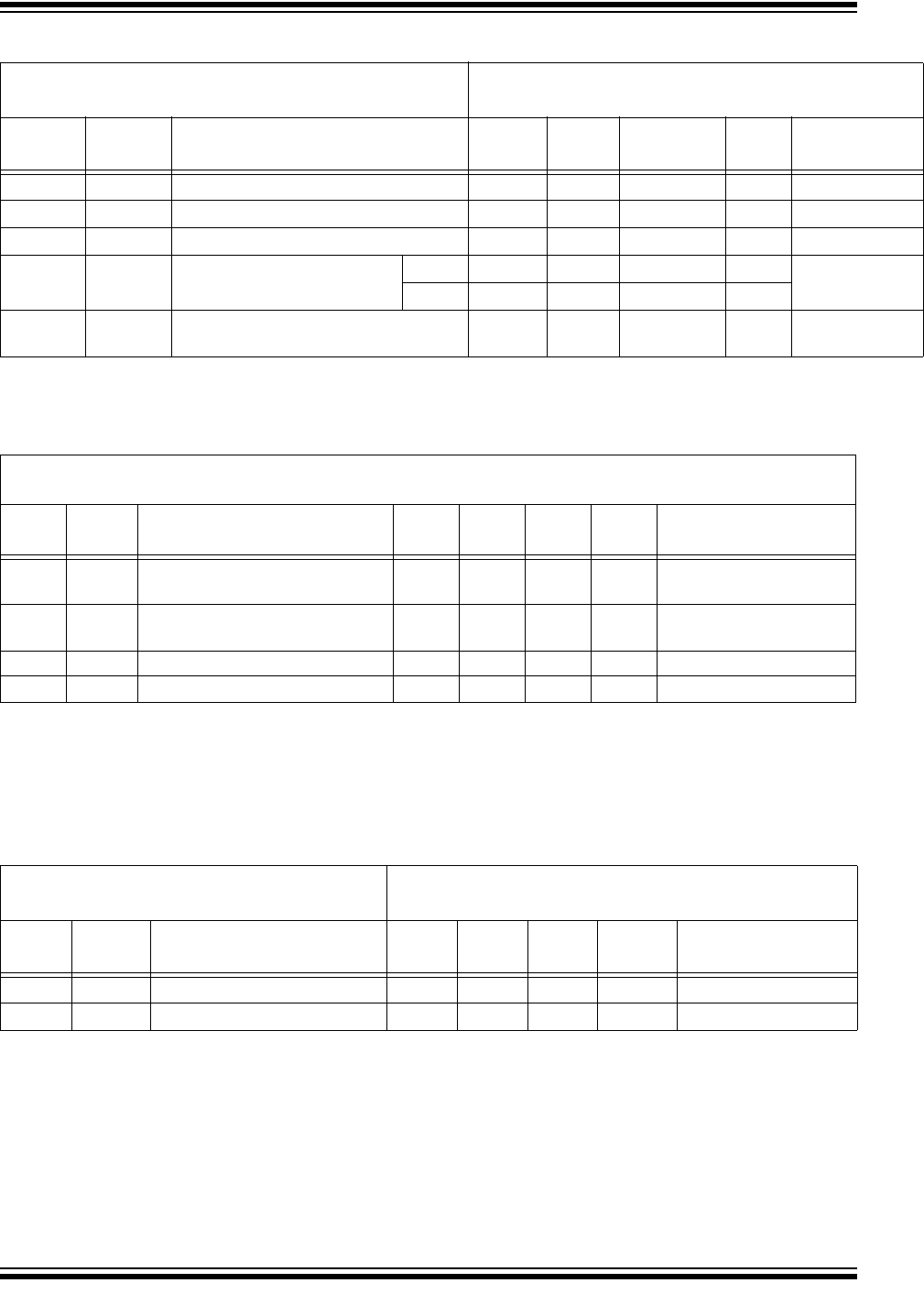
TABLE 17-7: COMPARATOR SPECIFICATIONS
TABLE 17-8: COMPARATOR VOLTAGE REFERENCE (CV
REF) SPECIFICATIONS
TABLE 17-9: VOLTAGE (VR) REFERENCE SPECIFICATIONS
Comparator Specifications
Standard Operating Conditions (unless otherwise stated)
Operating temperature -40°C ≤ T
A ≤ +125°C
Param.
No.
Sym. Characteristics Min. Typ. Max. Units Comments
CM01 V
OS Input Offset Voltage — ± 5.0 ± 10 mV
CM02 V
CM Input Common Mode Voltage 0 — VDD - 1.5 V
CM03* C
MRR Common Mode Rejection Ratio +55 — — db
CM04* T
RT Response Time Falling — 150 600 ns (Note 1)
Rising — 200 1000 ns
CM05* T
MC2COV Comparator Mode Change to Output
Valid
—— 10 μs
* These parameters are characterized but not tested.
Note 1: Response time is measured with one comparator input at (V
DD - 1.5)/2 - 100 mV to (VDD - 1.5)/2 + 20 mV.
Standard Operating Conditions (unless otherwise stated)
Operating temperature -40°C ≤ T
A ≤ +125°C
Param
No.
Sym. Characteristics Min. Typ† Max. Units Comments
CV01* CLSB Step Size
(2)
—
—
VDD/24
V
DD/32
—
—
V
V
Low Range (VRR = 1)
High Range (VRR = 0)
CV02* CACC Absolute Accuracy —
—
—
—
± 1/2
± 1/2
LSb
LSb
Low Range (VRR = 1)
High Range (VRR = 0)
CV03* C
R Unit Resistor Value (R) — 2k — Ω
CV04* CST Settling Time
(1)
——10μs
* These parameters are characterized but not tested.
† Data in “Typ” column is at 5V, 25°C unless otherwise stated. These parameters are for design
guidance only and are not tested.
Note 1: Settling time measured while VRR = 1 and VR<3:0> transitions from ‘0000’ to ‘1111’.
2: See Section 8.10 “Comparator Voltage Reference” for more information.
VR Voltage Reference Specifications
Standard Operating Conditions (unless otherwise stated)
Operating temperature -40°C ≤ T
A ≤ +125°C
Param
No.
Symbol Characteristics Min. Typ. Max. Units Comments
VR01 V
ROUT VR voltage output 0.5 0.6 0.7 V
VR02* T
STABLE Settling Time — 10 100* μs
* These parameters are characterized but not tested.