
Datasheet


Table Of Contents
- High-Performance RISC CPU:
- Special Microcontroller Features:
- Low-Power Features:
- Peripheral Features:
- PIC16F631 Pin Diagram
- PIC16F677 Pin Diagram
- PIC16F685 Pin Diagram
- PIC16F687/689 Pin Diagram
- PIC16F690 Pin Diagram (PDIP, SOIC, SSOP)
- PIC16F631/677/685/687/689/690 Pin Diagram (QFN)
- Most Current Data Sheet
- Errata
- Customer Notification System
- 1.0 Device Overview
- FIGURE 1-1: PIC16F631 Block Diagram
- FIGURE 1-2: PIC16F677 Block Diagram
- FIGURE 1-3: PIC16F685 Block Diagram
- FIGURE 1-4: PIC16F687/PIC16F689 Block Diagram
- FIGURE 1-5: PIC16F690 Block Diagram
- TABLE 1-1: Pinout Description - PIC16F631
- TABLE 1-2: Pinout Description - PIC16F677
- TABLE 1-3: Pinout Description - PIC16F685
- TABLE 1-4: Pinout Description - PIC16F687/PIC16F689
- TABLE 1-5: Pinout Description - PIC16F690
- 2.0 Memory Organization
- 2.1 Program Memory Organization
- 2.2 Data Memory Organization
- 2.2.1 General Purpose Register File
- 2.2.2 Special Function Registers
- FIGURE 2-4: PIC16F631 Special Function Registers
- FIGURE 2-5: PIC16F677 Special Function Registers
- FIGURE 2-6: PIC16F685 Special Function Registers
- FIGURE 2-7: PIC16F687/PIC16F689 Special Function Registers
- FIGURE 2-8: PIC16F690 Special Function Registers
- TABLE 2-1: PIC16F631/677/685/687/689/690 Special Function Registers Summary Bank 0
- TABLE 2-2: PIC16F631/677/685/687/689/690 Special Function Registers Summary Bank 1
- TABLE 2-3: PIC16F631/677/685/687/689/690 Special Function Registers Summary Bank 2
- TABLE 2-4: PIC16F631/677/685/687/689/690 Special Function Registers Summary Bank 3
- Register 2-1: STATUS: STATUS Register
- Register 2-2: OPTION_REG: Option Register
- Register 2-3: INTCON: Interrupt Control Register
- Register 2-4: PIE1: Peripheral Interrupt Enable Register 1
- Register 2-5: PIE2: Peripheral Interrupt Enable Register 2
- Register 2-6: PIR1: Peripheral Interrupt Request Register 1
- Register 2-7: PIR2: Peripheral Interrupt Request Register 2
- Register 2-8: PCON: Power Control Register
- 2.3 PCL and PCLATH
- 2.4 Indirect Addressing, INDF and FSR Registers
- 3.0 Oscillator Module (With Fail-Safe Clock Monitor)
- 4.0 I/O Ports
- 4.1 PORTA and the TRISA Registers
- 4.2 Additional Pin Functions
- 4.3 PORTB and TRISB Registers
- 4.4 Additional PORTB Pin Functions
- 4.5 PORTC and TRISC Registers
- 5.0 Timer0 Module
- 6.0 Timer1 Module with Gate Control
- 6.1 Timer1 Operation
- 6.2 Clock Source Selection
- 6.3 Timer1 Prescaler
- 6.4 Timer1 Oscillator
- 6.5 Timer1 Operation in Asynchronous Counter Mode
- 6.6 Timer1 Gate
- 6.7 Timer1 Interrupt
- 6.8 Timer1 Operation During Sleep
- 6.9 ECCP Capture/Compare Time Base
- 6.10 ECCP Special Event Trigger
- 6.11 Comparator Synchronization
- 6.12 Timer1 Control Register
- 7.0 Timer2 Module
- 8.0 Comparator Module
- 8.1 Comparator Overview
- 8.2 Comparator Control
- 8.3 Comparator Response Time
- 8.4 Comparator Interrupt Operation
- 8.5 Operation During Sleep
- 8.6 Effects of a Reset
- 8.7 Analog Input Connection Considerations
- 8.8 Additional Comparator Features
- 8.9 Comparator SR Latch
- 8.10 Comparator Voltage Reference
- 9.0 Analog-to-Digital Converter (ADC) Module
- FIGURE 9-1: ADC Block Diagram
- 9.1 ADC Configuration
- 9.2 ADC Operation
- 9.2.1 Starting A Conversion
- 9.2.2 Completion of a Conversion
- 9.2.3 Terminating a conversion
- 9.2.4 ADC Operation During Sleep
- 9.2.5 SPecial Event Trigger
- 9.2.6 A/D Conversion Procedure
- 9.2.7 ADC Register Definitions
- Register 9-1: ADCON0: A/D Control Register 0
- Register 9-2: ADCON1: A/D Control Register 1
- Register 9-3: ADRESH: ADC Result Register High (ADRESH) ADFM = 0
- Register 9-4: ADRESL: ADC Result Register Low (ADRESL) ADFM = 0
- Register 9-5: ADRESH: ADC Result Register High (ADRESH) ADFM = 1
- Register 9-6: ADRESL: ADC Result Register Low (ADRESL) ADFM = 1
- 9.3 A/D Acquisition Requirements
- 10.0 Data EEPROM and Flash Program Memory Control
- 10.1 EEADR and EEADRH Registers
- 10.2 Write Verify
- 10.3 Protection Against Spurious Write
- 10.4 Data EEPROM Operation During Code-Protect
- 11.0 Enhanced Capture/Compare/PWM Module
- TABLE 11-1: ECCP Mode - Timer Resources Required
- Register 11-1: CCP1CON: Enhanced CCP1 Control Register
- 11.1 Capture Mode
- 11.2 Compare Mode
- 11.3 PWM Mode
- 11.4 PWM (Enhanced Mode)
- FIGURE 11-5: Example Simplified Block Diagram of the Enhanced PWM Mode
- TABLE 11-4: example Pin Assignments for Various PWM Enhanced Modes
- FIGURE 11-6: Example PWM (enhanced Mode) Output Relationships (Active-High State)
- FIGURE 11-7: Example Enhanced PWM Output Relationships (Active-Low State)
- 11.4.1 Half-Bridge Mode
- 11.4.2 Full-Bridge Mode
- 11.4.3 Start-up Considerations
- 11.4.4 Enhanced PWM Auto-shutdown mode
- 11.4.5 Auto-Restart Mode
- 11.4.6 Programmable Dead-Band Delay mode
- 11.4.7 Pulse Steering Mode
- Register 11-4: PSTRCON: Pulse Steering Control Register(1)
- FIGURE 11-19: Simplified Steering Block Diagram
- FIGURE 11-20: Example of Steering Event at End of Instruction (STRSYNC = 0)
- FIGURE 11-21: Example of Steering Event at Beginning of Instruction (STRSYNC = 1)
- TABLE 11-5: Summary of Registers Associated with Capture, Compare and PWM
- 12.0 Enhanced Universal Synchronous Asynchronous Receiver Transmitter (EUSART)
- FIGURE 12-1: EUSART Transmit Block Diagram
- FIGURE 12-2: EUSART Receive Block Diagram
- 12.1 EUSART Asynchronous Mode
- 12.2 Clock Accuracy with Asynchronous Operation
- 12.3 EUSART Baud Rate Generator (BRG)
- 12.4 EUSART Synchronous Mode
- 12.5 EUSART Operation During Sleep
- 13.0 SSP Module Overview
- 13.1 SPI Mode
- 13.2 Operation
- 13.3 Enabling SPI I/O
- 13.4 Typical Connection
- 13.5 Master Mode
- 13.6 Slave Mode
- 13.7 Slave Select Synchronization
- 13.8 Sleep Operation
- 13.9 Effects of a Reset
- 13.10 Bus Mode Compatibility
- 13.11 SSP I2C Operation
- 13.12 Slave Mode
- 13.13 Master Mode
- 13.14 Multi-Master Mode
- 14.0 Special Features of the CPU
- 14.1 Configuration Bits
- 14.2 Reset
- FIGURE 14-1: Simplified Block Diagram of On-chip Reset Circuit
- 14.2.1 Power-on Reset (POR)
- 14.2.2 MCLR
- 14.2.3 Power-up Timer (PWRT)
- 14.2.4 Brown-out Reset (BOR)
- 14.2.5 Time-out Sequence
- 14.2.6 Power Control (PCON) Register
- TABLE 14-1: Time-out in Various Situations
- TABLE 14-2: Status/PCON Bits and Their Significance
- TABLE 14-3: Summary of Registers Associated with Brown-out
- FIGURE 14-4: Time-out Sequence On Power-up (Delayed MCLR): Case 1
- FIGURE 14-5: Time-out Sequence On Power-up (Delayed MCLR): Case 2
- FIGURE 14-6: Time-out Sequence on Power-up (MCLR with Vdd)
- TABLE 14-4: Initialization Condition for Register
- TABLE 14-5: Initialization Condition for Special Registers
- 14.3 Interrupts
- 14.4 Context Saving During Interrupts
- 14.5 Watchdog Timer (WDT)
- 14.6 Power-Down Mode (Sleep)
- 14.7 Code Protection
- 14.8 ID Locations
- 14.9 In-Circuit Serial Programming
- 15.0 Instruction Set Summary
- 16.0 Development Support
- 16.1 MPLAB Integrated Development Environment Software
- 16.2 MPASM Assembler
- 16.3 MPLAB C18 and MPLAB C30 C Compilers
- 16.4 MPLINK Object Linker/ MPLIB Object Librarian
- 16.5 MPLAB ASM30 Assembler, Linker and Librarian
- 16.6 MPLAB SIM Software Simulator
- 16.7 MPLAB ICE 2000 High-Performance In-Circuit Emulator
- 16.8 MPLAB REAL ICE In-Circuit Emulator System
- 16.9 MPLAB ICD 2 In-Circuit Debugger
- 16.10 MPLAB PM3 Device Programmer
- 16.11 PICSTART Plus Development Programmer
- 16.12 PICkit 2 Development Programmer
- 16.13 Demonstration, Development and Evaluation Boards
- 17.0 Electrical Specifications
- Absolute Maximum Ratings(†)
- 17.1 DC Characteristics: PIC16F631/677/685/687/689/690-I (Industrial) PIC16F631/677/685/687/689/690-E (Extended)
- 17.2 DC Characteristics: PIC16F631/677/685/687/689/690-I (Industrial) PIC16F631/677/685/687/689/690-E (Extended)
- 17.3 DC Characteristics: PIC16F631/677/685/687/689/690-E (Extended)
- 17.4 DC Characteristics: PIC16F631/677/685/687/689/690-I (Industrial) PIC16F631/677/685/687/689/690-E (Extended)
- 17.5 Thermal Considerations
- 17.6 Timing Parameter Symbology
- 17.7 AC Characteristics: PIC16F631/677/685/687/689/690 (Industrial, Extended)
- FIGURE 17-4: Clock Timing
- TABLE 17-1: Clock Oscillator Timing Requirements
- TABLE 17-2: Oscillator Parameters
- FIGURE 17-5: CLKOUT and I/O Timing
- TABLE 17-3: CLKOUT and I/O Timing Parameters
- FIGURE 17-6: Reset, Watchdog Timer, Oscillator Start-up Timer and Power-up Timer Timing
- FIGURE 17-7: Brown-out Reset Timing and Characteristics
- TABLE 17-4: Reset, Watchdog Timer, Oscillator Start-up Timer, Power-up Timer and Brown-out Reset Parameters
- FIGURE 17-8: Timer0 and Timer1 External Clock Timings
- TABLE 17-5: Timer0 and Timer1 External Clock Requirements
- FIGURE 17-9: Capture/Compare/PWM Timings (ECCP)
- TABLE 17-6: Capture/Compare/PWM Requirements (ECCP)
- TABLE 17-7: Comparator Specifications
- TABLE 17-8: Comparator Voltage Reference (CVref) Specifications
- TABLE 17-9: Voltage (VR) Reference Specifications
- FIGURE 17-10: EUSART Synchronous Transmission (Master/Slave) Timing
- TABLE 17-10: EUSART Synchronous Transmission Requirements
- FIGURE 17-11: EUSART Synchronous Receive (Master/Slave) Timing
- TABLE 17-11: EUSART Synchronous Receive Requirements
- FIGURE 17-12: SPI Master Mode Timing (CKE = 0, SMP = 0)
- FIGURE 17-13: SPI Master Mode Timing (CKE = 1, SMP = 1)
- FIGURE 17-14: SPI Slave Mode Timing (CKE = 0)
- FIGURE 17-15: SPI Slave Mode Timing (CKE = 1)
- TABLE 17-12: SPI Mode requirements
- FIGURE 17-16: I2C™ Bus Start/Stop Bits Timing
- TABLE 17-13: I2C™ Bus Start/Stop Bits Requirements
- FIGURE 17-17: I2C™ Bus Data Timing
- TABLE 17-14: I2C™ Bus Data Requirements
- TABLE 17-15: A/D Converter (ADC) Characteristics:
- FIGURE 17-18: A/D Conversion Timing (Normal Mode)
- TABLE 17-16: A/D Conversion Requirements
- FIGURE 17-19: A/D Conversion Timing (Sleep Mode)
- 18.0 DC and AC Characteristics Graphs and Tables
- FIGURE 18-1: Typical Idd vs. Fosc Over Vdd (EC Mode)
- FIGURE 18-2: Maximum Idd vs. Fosc Over Vdd (EC Mode)
- FIGURE 18-3: Typical Idd vs. Fosc Over Vdd (HS Mode)
- FIGURE 18-4: Maximum Idd vs. Fosc Over Vdd (HS Mode)
- FIGURE 18-5: Typical Idd vs. Vdd Over Fosc (XT Mode)
- FIGURE 18-6: Maximum Idd vs. Vdd Over Fosc (XT Mode)
- FIGURE 18-7: Idd vs. Vdd (LP Mode)
- FIGURE 18-8: Typical Idd vs. Vdd Over Fosc (EXTRC Mode)
- FIGURE 18-9: Maximum Idd vs. Vdd Over Fosc (EXTRC Mode)
- FIGURE 18-10: Idd vs. Vdd Over Fosc (LFINTOSC Mode, 31 kHz)
- FIGURE 18-11: Typical Idd vs. Fosc Over Vdd (HFINTOSC Mode)
- FIGURE 18-12: Maximum Idd vs. Fosc Over Vdd (HFINTOSC Mode)
- FIGURE 18-13: Typical Ipd vs. Vdd (Sleep Mode, all Peripherals Disabled)
- FIGURE 18-14: Maximum Ipd vs. Vdd (Sleep Mode, all Peripherals Disabled)
- FIGURE 18-15: Comparator Ipd vs. Vdd (Both Comparators Enabled)
- FIGURE 18-16: BOR Ipd VS. Vdd Over Temperature
- FIGURE 18-17: Typical WDT Ipd VS. Vdd Over Temperature
- FIGURE 18-18: Maximum WDT Ipd VS. Vdd Over Temperature
- FIGURE 18-19: WDT Period VS. Vdd Over Temperature
- FIGURE 18-20: WDT Period VS. Temperature Over Vdd (5.0V)
- FIGURE 18-21: CVref Ipd VS. Vdd Over Temperature (High Range)
- FIGURE 18-22: CVref Ipd VS. Vdd Over Temperature (Low Range)
- FIGURE 18-23: Typical VP6 Reference Ipd vs. Vdd (25 C)
- FIGURE 18-24: Maximum VP6 Reference Ipd vs. Vdd Over Temperature
- FIGURE 18-25: T1OSC Ipd vs. Vdd Over Temperature (32 kHz)
- FIGURE 18-26: Vol VS. Iol Over Temperature (Vdd = 3.0V)
- FIGURE 18-27: Vol VS. Iol Over Temperature (Vdd = 5.0V)
- FIGURE 18-28: Voh VS. Ioh Over Temperature (Vdd = 3.0V)
- FIGURE 18-29: Voh VS. Ioh Over Temperature (Vdd = 5.0V)
- FIGURE 18-30: TTL Input Threshold Vin VS. Vdd Over Temperature
- FIGURE 18-31: Schmitt Trigger Input Threshold Vin VS. Vdd Over Temperature
- FIGURE 18-32: Comparator Response Time (Rising Edge)
- FIGURE 18-33: Comparator Response Time (Falling Edge)
- FIGURE 18-34: LFINTOSC Frequency vs. Vdd Over Temperature (31 kHz)
- FIGURE 18-35: ADC Clock Period vs. Vdd Over Temperature
- FIGURE 18-36: Typical HFINTOSC Start-Up Times vs. Vdd Over Temperature
- FIGURE 18-37: Maximum HFINTOSC Start-Up Times vs. Vdd Over Temperature
- FIGURE 18-38: Minimum HFINTOSC Start-Up Times vs. Vdd Over Temperature
- FIGURE 18-39: Typical HFINTOSC Frequency Change vs. Vdd (25 C)
- FIGURE 18-40: Typical HFINTOSC Frequency Change Over Device Vdd (85 C)
- FIGURE 18-41: Typical HFINTOSC Frequency Change vs. Vdd (125 C)
- FIGURE 18-42: Typical HFINTOSC Frequency Change vs. Vdd (-40 C)
- FIGURE 18-43: Typical VP6 Reference Voltage vs. Vdd (25 C)
- FIGURE 18-44: Typical VP6 Reference Voltage Over Temperature (3V)
- FIGURE 18-45: Typical VP6 Reference Voltage Over Temperature (5V)
- FIGURE 18-46: Typical VP6 Reference Voltage Distribution (3V, 25 C)
- FIGURE 18-47: Typical VP6 Reference Voltage Distribution (3V, 85 C)
- FIGURE 18-48: Typical VP6 Reference Voltage Distribution (3V, 125 C)
- FIGURE 18-49: Typical VP6 Reference Voltage Distribution (3V, -40 C)
- FIGURE 18-50: Typical VP6 Reference Voltage Distribution (5V, 25 C)
- FIGURE 18-51: Typical VP6 Reference Voltage Distribution (5V, 85 C)
- FIGURE 18-52: Typical VP6 Reference Voltage Distribution (5V, 125 C)
- FIGURE 18-53: Typical VP6 Reference Voltage Distribution (5V, -40 C)
- 19.0 Packaging Information
- Appendix A: Data Sheet Revision History
- Appendix B: Migrating from other PIC® Devices
- INDEX
- The Microchip Web Site
- Customer Change Notification Service
- Customer Support
- Reader Response
- Product Identification System
- Worldwide Sales
© 2008 Microchip Technology Inc. DS41262E-page 169
PIC16F631/677/685/687/689/690
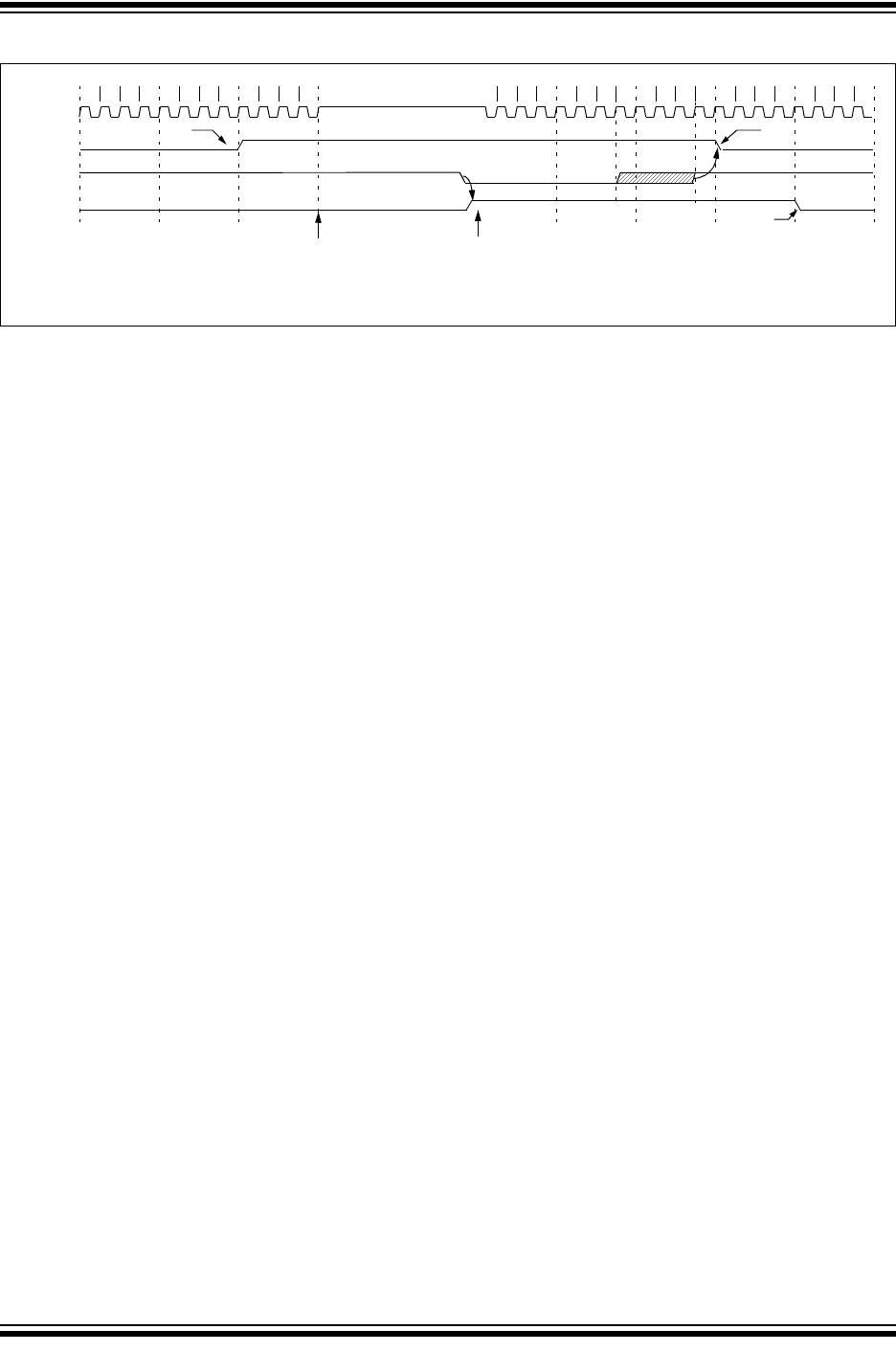
FIGURE 12-8: AUTO-WAKE-UP BIT (WUE) TIMINGS DURING SLEEP
12.3.3 BREAK CHARACTER SEQUENCE
The EUSART module has the capability of sending the
special Break character sequences that are required by
the LIN bus standard. A Break character consists of a
Start bit, followed by 12 ‘0’ bits and a Stop bit.
To send a Break character, set the SENDB and TXEN
bits of the TXSTA register. The Break character trans-
mission is then initiated by a write to the TXREG. The
value of data written to TXREG will be ignored and all
‘0’s will be transmitted.
The SENDB bit is automatically reset by hardware after
the corresponding Stop bit is sent. This allows the user
to preload the transmit FIFO with the next transmit byte
following the Break character (typically, the Sync
character in the LIN specification).
The TRMT bit of the TXSTA register indicates when the
transmit operation is active or Idle, just as it does during
normal transmission. See Figure 12-9 for the timing of
the Break character sequence.
12.3.3.1 Break and Sync Transmit Sequence
The following sequence will start a message frame
header made up of a Break, followed by an auto-baud
Sync byte. This sequence is typical of a LIN bus
master.
1. Configure the EUSART for the desired mode.
2. Set the TXEN and SENDB bits to enable the
Break sequence.
3. Load the TXREG with a dummy character to
initiate transmission (the value is ignored).
4. Write ‘55h’ to TXREG to load the Sync character
into the transmit FIFO buffer.
5. After the Break has been sent, the SENDB bit is
reset by hardware and the Sync character is
then transmitted.
When the TXREG becomes empty, as indicated by the
TXIF, the next data byte can be written to TXREG.
12.3.4 RECEIVING A BREAK CHARACTER
The Enhanced EUSART module can receive a Break
character in two ways.
The first method to detect a Break character uses the
FERR bit of the RCSTA register and the Received data
as indicated by RCREG. The Baud Rate Generator is
assumed to have been initialized to the expected baud
rate.
A Break character has been received when;
• RCIF bit is set
• FERR bit is set
• RCREG = 00h
The second method uses the Auto-Wake-up feature
described in Section 12.3.2 “Auto-Wake-up on
Break”. By enabling this feature, the EUSART will
sample the next two transitions on RX/DT, cause an
RCIF interrupt, and receive the next data byte followed
by another interrupt.
Note that following a Break character, the user will
typically want to enable the Auto-Baud Detect feature.
For both methods, the user can set the ABDEN bit of
the BAUDCTL register before placing the EUSART in
Sleep mode.
Q1Q2 Q3 Q4 Q1Q2 Q3 Q4 Q1 Q2 Q3
Q4
Q1 Q2 Q3 Q4 Q1 Q2 Q3 Q4 Q1 Q2 Q3 Q4 Q1 Q2 Q3 Q4 Q1 Q2 Q3 Q4
OSC1
WUE bit
RX/DT Line
RCIF
Bit Set by User
Auto Cleared
Cleared due to User Read of RCREG
Sleep Command Executed
Note 1
Note 1: If the wake-up event requires long oscillator warm-up time, the automatic clearing of the WUE bit can occur while the stposc signal is
still active. This sequence should not depend on the presence of Q clocks.
2: The EUSART remains in Idle while the WUE bit is set.
Sleep Ends