
Information
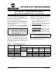

2010 Microchip Technology Inc. DS80243M-page 9
PIC16F631/677/685/687/689/690
4. Module: Analog-To-Digital Converter
(ADC) Module
(PIC16F685/687/689/690 Only)
Selecting the VP6 reference as the analog input
source (CHS<3:0> = 1101) for the ADC conversion
after sampling another analog channel with input
voltages approximately greater than 1.2V can
temporarily disturb the HFINTOSC oscillator.
Work around
Select an ADC channel with input voltages lower
than 1.2V prior to selecting the VP6 reference
voltage input. Any analog channel can be used,
even if that channel is configured as a digital I/O
(configured as an output) that is driving the output
pin low. An alternative is to configure the CV
REF
module to output a voltage less than 1.2V and then
selecting that analog channel CHS<3:0> = 1100
as the analog input source.
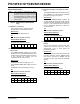
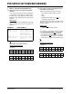
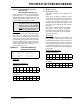
EXAMPLE 2: AVOID DISTURBING THE
HFINTOSC OSCILLATOR
Silicon Fix
None.
Affected Silicon Revisions
PIC16F677
PIC16F685/PIC16F687/PIC16F689/
PIC16F690
5. Module: Timer1
5.1 Asynchronous Timer1
This Errata supersedes Errata DS80233 and
DS80329.
When TImer1 is started or updated, the timer
needs to see a falling edge from the external clock
source before a rising edge can increment the
counter. If writes to TMR1H and TMR1L are not
completed while the external clock pulse is still
high, Timer1 will not count the first clock pulse after
the update.
When using an external crystal, the pulse width
from rising to falling edge is temperature
dependent and may decrease with temperature.
As a result, the timer may require an additional
oscillation to overflow.
Work around
Switching to the HFINTOSC after reloading, the
timer ensures the Timer1 will see a falling edge
before switching back to the external clock source.
Due to the time from Timer1 overflow to the reload
being application specific, wait for the timer to
increment before beginning the reload sequence.
This ensures the timer does not miss a rising edge
during reload.
Affected Silicon Revisions
PIC16F631/PIC16F677
PIC16F685/PIC16F687/PIC16F689/
PIC16F690
Note: This only occurs when selecting the
VP6 reference ADC channel using the
CHS<3:0> bits in the ADCON0
register and NOT during the start of an
actual ADC conversion using the GO/
DONE
bit in the ADCON0 register.
A1
X
A3 A4 A5
A6
XXX
X
BANKSEL ADCON0 ;
MOVLW B’XX110001’ ;Select ADC
MOVWF ADCON0 ;Channel CV
REF
MOVLW B’XX110101’ ;Select ADC
MOVWF ADCON0 ;Channel VP6
A1
X
A3 A4 A5
A6
XXX
X