
Datasheet


Table Of Contents
- High-Performance RISC CPU:
- Special Microcontroller Features:
- Low-Power Features:
- Peripheral Features:
- PIC16F631 Pin Diagram
- PIC16F677 Pin Diagram
- PIC16F685 Pin Diagram
- PIC16F687/689 Pin Diagram
- PIC16F690 Pin Diagram (PDIP, SOIC, SSOP)
- PIC16F631/677/685/687/689/690 Pin Diagram (QFN)
- Most Current Data Sheet
- Errata
- Customer Notification System
- 1.0 Device Overview
- FIGURE 1-1: PIC16F631 Block Diagram
- FIGURE 1-2: PIC16F677 Block Diagram
- FIGURE 1-3: PIC16F685 Block Diagram
- FIGURE 1-4: PIC16F687/PIC16F689 Block Diagram
- FIGURE 1-5: PIC16F690 Block Diagram
- TABLE 1-1: Pinout Description - PIC16F631
- TABLE 1-2: Pinout Description - PIC16F677
- TABLE 1-3: Pinout Description - PIC16F685
- TABLE 1-4: Pinout Description - PIC16F687/PIC16F689
- TABLE 1-5: Pinout Description - PIC16F690
- 2.0 Memory Organization
- 2.1 Program Memory Organization
- 2.2 Data Memory Organization
- 2.2.1 General Purpose Register File
- 2.2.2 Special Function Registers
- FIGURE 2-4: PIC16F631 Special Function Registers
- FIGURE 2-5: PIC16F677 Special Function Registers
- FIGURE 2-6: PIC16F685 Special Function Registers
- FIGURE 2-7: PIC16F687/PIC16F689 Special Function Registers
- FIGURE 2-8: PIC16F690 Special Function Registers
- TABLE 2-1: PIC16F631/677/685/687/689/690 Special Function Registers Summary Bank 0
- TABLE 2-2: PIC16F631/677/685/687/689/690 Special Function Registers Summary Bank 1
- TABLE 2-3: PIC16F631/677/685/687/689/690 Special Function Registers Summary Bank 2
- TABLE 2-4: PIC16F631/677/685/687/689/690 Special Function Registers Summary Bank 3
- Register 2-1: STATUS: STATUS Register
- Register 2-2: OPTION_REG: Option Register
- Register 2-3: INTCON: Interrupt Control Register
- Register 2-4: PIE1: Peripheral Interrupt Enable Register 1
- Register 2-5: PIE2: Peripheral Interrupt Enable Register 2
- Register 2-6: PIR1: Peripheral Interrupt Request Register 1
- Register 2-7: PIR2: Peripheral Interrupt Request Register 2
- Register 2-8: PCON: Power Control Register
- 2.3 PCL and PCLATH
- 2.4 Indirect Addressing, INDF and FSR Registers
- 3.0 Oscillator Module (With Fail-Safe Clock Monitor)
- 4.0 I/O Ports
- 4.1 PORTA and the TRISA Registers
- 4.2 Additional Pin Functions
- 4.3 PORTB and TRISB Registers
- 4.4 Additional PORTB Pin Functions
- 4.5 PORTC and TRISC Registers
- 5.0 Timer0 Module
- 6.0 Timer1 Module with Gate Control
- 6.1 Timer1 Operation
- 6.2 Clock Source Selection
- 6.3 Timer1 Prescaler
- 6.4 Timer1 Oscillator
- 6.5 Timer1 Operation in Asynchronous Counter Mode
- 6.6 Timer1 Gate
- 6.7 Timer1 Interrupt
- 6.8 Timer1 Operation During Sleep
- 6.9 ECCP Capture/Compare Time Base
- 6.10 ECCP Special Event Trigger
- 6.11 Comparator Synchronization
- 6.12 Timer1 Control Register
- 7.0 Timer2 Module
- 8.0 Comparator Module
- 8.1 Comparator Overview
- 8.2 Comparator Control
- 8.3 Comparator Response Time
- 8.4 Comparator Interrupt Operation
- 8.5 Operation During Sleep
- 8.6 Effects of a Reset
- 8.7 Analog Input Connection Considerations
- 8.8 Additional Comparator Features
- 8.9 Comparator SR Latch
- 8.10 Comparator Voltage Reference
- 9.0 Analog-to-Digital Converter (ADC) Module
- FIGURE 9-1: ADC Block Diagram
- 9.1 ADC Configuration
- 9.2 ADC Operation
- 9.2.1 Starting A Conversion
- 9.2.2 Completion of a Conversion
- 9.2.3 Terminating a conversion
- 9.2.4 ADC Operation During Sleep
- 9.2.5 SPecial Event Trigger
- 9.2.6 A/D Conversion Procedure
- 9.2.7 ADC Register Definitions
- Register 9-1: ADCON0: A/D Control Register 0
- Register 9-2: ADCON1: A/D Control Register 1
- Register 9-3: ADRESH: ADC Result Register High (ADRESH) ADFM = 0
- Register 9-4: ADRESL: ADC Result Register Low (ADRESL) ADFM = 0
- Register 9-5: ADRESH: ADC Result Register High (ADRESH) ADFM = 1
- Register 9-6: ADRESL: ADC Result Register Low (ADRESL) ADFM = 1
- 9.3 A/D Acquisition Requirements
- 10.0 Data EEPROM and Flash Program Memory Control
- 10.1 EEADR and EEADRH Registers
- 10.2 Write Verify
- 10.3 Protection Against Spurious Write
- 10.4 Data EEPROM Operation During Code-Protect
- 11.0 Enhanced Capture/Compare/PWM Module
- TABLE 11-1: ECCP Mode - Timer Resources Required
- Register 11-1: CCP1CON: Enhanced CCP1 Control Register
- 11.1 Capture Mode
- 11.2 Compare Mode
- 11.3 PWM Mode
- 11.4 PWM (Enhanced Mode)
- FIGURE 11-5: Example Simplified Block Diagram of the Enhanced PWM Mode
- TABLE 11-4: example Pin Assignments for Various PWM Enhanced Modes
- FIGURE 11-6: Example PWM (enhanced Mode) Output Relationships (Active-High State)
- FIGURE 11-7: Example Enhanced PWM Output Relationships (Active-Low State)
- 11.4.1 Half-Bridge Mode
- 11.4.2 Full-Bridge Mode
- 11.4.3 Start-up Considerations
- 11.4.4 Enhanced PWM Auto-shutdown mode
- 11.4.5 Auto-Restart Mode
- 11.4.6 Programmable Dead-Band Delay mode
- 11.4.7 Pulse Steering Mode
- Register 11-4: PSTRCON: Pulse Steering Control Register(1)
- FIGURE 11-19: Simplified Steering Block Diagram
- FIGURE 11-20: Example of Steering Event at End of Instruction (STRSYNC = 0)
- FIGURE 11-21: Example of Steering Event at Beginning of Instruction (STRSYNC = 1)
- TABLE 11-5: Summary of Registers Associated with Capture, Compare and PWM
- 12.0 Enhanced Universal Synchronous Asynchronous Receiver Transmitter (EUSART)
- FIGURE 12-1: EUSART Transmit Block Diagram
- FIGURE 12-2: EUSART Receive Block Diagram
- 12.1 EUSART Asynchronous Mode
- 12.2 Clock Accuracy with Asynchronous Operation
- 12.3 EUSART Baud Rate Generator (BRG)
- 12.4 EUSART Synchronous Mode
- 12.5 EUSART Operation During Sleep
- 13.0 SSP Module Overview
- 13.1 SPI Mode
- 13.2 Operation
- 13.3 Enabling SPI I/O
- 13.4 Typical Connection
- 13.5 Master Mode
- 13.6 Slave Mode
- 13.7 Slave Select Synchronization
- 13.8 Sleep Operation
- 13.9 Effects of a Reset
- 13.10 Bus Mode Compatibility
- 13.11 SSP I2C Operation
- 13.12 Slave Mode
- 13.13 Master Mode
- 13.14 Multi-Master Mode
- 14.0 Special Features of the CPU
- 14.1 Configuration Bits
- 14.2 Reset
- FIGURE 14-1: Simplified Block Diagram of On-chip Reset Circuit
- 14.2.1 Power-on Reset (POR)
- 14.2.2 MCLR
- 14.2.3 Power-up Timer (PWRT)
- 14.2.4 Brown-out Reset (BOR)
- 14.2.5 Time-out Sequence
- 14.2.6 Power Control (PCON) Register
- TABLE 14-1: Time-out in Various Situations
- TABLE 14-2: Status/PCON Bits and Their Significance
- TABLE 14-3: Summary of Registers Associated with Brown-out
- FIGURE 14-4: Time-out Sequence On Power-up (Delayed MCLR): Case 1
- FIGURE 14-5: Time-out Sequence On Power-up (Delayed MCLR): Case 2
- FIGURE 14-6: Time-out Sequence on Power-up (MCLR with Vdd)
- TABLE 14-4: Initialization Condition for Register
- TABLE 14-5: Initialization Condition for Special Registers
- 14.3 Interrupts
- 14.4 Context Saving During Interrupts
- 14.5 Watchdog Timer (WDT)
- 14.6 Power-Down Mode (Sleep)
- 14.7 Code Protection
- 14.8 ID Locations
- 14.9 In-Circuit Serial Programming
- 15.0 Instruction Set Summary
- 16.0 Development Support
- 16.1 MPLAB Integrated Development Environment Software
- 16.2 MPASM Assembler
- 16.3 MPLAB C18 and MPLAB C30 C Compilers
- 16.4 MPLINK Object Linker/ MPLIB Object Librarian
- 16.5 MPLAB ASM30 Assembler, Linker and Librarian
- 16.6 MPLAB SIM Software Simulator
- 16.7 MPLAB ICE 2000 High-Performance In-Circuit Emulator
- 16.8 MPLAB REAL ICE In-Circuit Emulator System
- 16.9 MPLAB ICD 2 In-Circuit Debugger
- 16.10 MPLAB PM3 Device Programmer
- 16.11 PICSTART Plus Development Programmer
- 16.12 PICkit 2 Development Programmer
- 16.13 Demonstration, Development and Evaluation Boards
- 17.0 Electrical Specifications
- Absolute Maximum Ratings(†)
- 17.1 DC Characteristics: PIC16F631/677/685/687/689/690-I (Industrial) PIC16F631/677/685/687/689/690-E (Extended)
- 17.2 DC Characteristics: PIC16F631/677/685/687/689/690-I (Industrial) PIC16F631/677/685/687/689/690-E (Extended)
- 17.3 DC Characteristics: PIC16F631/677/685/687/689/690-E (Extended)
- 17.4 DC Characteristics: PIC16F631/677/685/687/689/690-I (Industrial) PIC16F631/677/685/687/689/690-E (Extended)
- 17.5 Thermal Considerations
- 17.6 Timing Parameter Symbology
- 17.7 AC Characteristics: PIC16F631/677/685/687/689/690 (Industrial, Extended)
- FIGURE 17-4: Clock Timing
- TABLE 17-1: Clock Oscillator Timing Requirements
- TABLE 17-2: Oscillator Parameters
- FIGURE 17-5: CLKOUT and I/O Timing
- TABLE 17-3: CLKOUT and I/O Timing Parameters
- FIGURE 17-6: Reset, Watchdog Timer, Oscillator Start-up Timer and Power-up Timer Timing
- FIGURE 17-7: Brown-out Reset Timing and Characteristics
- TABLE 17-4: Reset, Watchdog Timer, Oscillator Start-up Timer, Power-up Timer and Brown-out Reset Parameters
- FIGURE 17-8: Timer0 and Timer1 External Clock Timings
- TABLE 17-5: Timer0 and Timer1 External Clock Requirements
- FIGURE 17-9: Capture/Compare/PWM Timings (ECCP)
- TABLE 17-6: Capture/Compare/PWM Requirements (ECCP)
- TABLE 17-7: Comparator Specifications
- TABLE 17-8: Comparator Voltage Reference (CVref) Specifications
- TABLE 17-9: Voltage (VR) Reference Specifications
- FIGURE 17-10: EUSART Synchronous Transmission (Master/Slave) Timing
- TABLE 17-10: EUSART Synchronous Transmission Requirements
- FIGURE 17-11: EUSART Synchronous Receive (Master/Slave) Timing
- TABLE 17-11: EUSART Synchronous Receive Requirements
- FIGURE 17-12: SPI Master Mode Timing (CKE = 0, SMP = 0)
- FIGURE 17-13: SPI Master Mode Timing (CKE = 1, SMP = 1)
- FIGURE 17-14: SPI Slave Mode Timing (CKE = 0)
- FIGURE 17-15: SPI Slave Mode Timing (CKE = 1)
- TABLE 17-12: SPI Mode requirements
- FIGURE 17-16: I2C™ Bus Start/Stop Bits Timing
- TABLE 17-13: I2C™ Bus Start/Stop Bits Requirements
- FIGURE 17-17: I2C™ Bus Data Timing
- TABLE 17-14: I2C™ Bus Data Requirements
- TABLE 17-15: A/D Converter (ADC) Characteristics:
- FIGURE 17-18: A/D Conversion Timing (Normal Mode)
- TABLE 17-16: A/D Conversion Requirements
- FIGURE 17-19: A/D Conversion Timing (Sleep Mode)
- 18.0 DC and AC Characteristics Graphs and Tables
- FIGURE 18-1: Typical Idd vs. Fosc Over Vdd (EC Mode)
- FIGURE 18-2: Maximum Idd vs. Fosc Over Vdd (EC Mode)
- FIGURE 18-3: Typical Idd vs. Fosc Over Vdd (HS Mode)
- FIGURE 18-4: Maximum Idd vs. Fosc Over Vdd (HS Mode)
- FIGURE 18-5: Typical Idd vs. Vdd Over Fosc (XT Mode)
- FIGURE 18-6: Maximum Idd vs. Vdd Over Fosc (XT Mode)
- FIGURE 18-7: Idd vs. Vdd (LP Mode)
- FIGURE 18-8: Typical Idd vs. Vdd Over Fosc (EXTRC Mode)
- FIGURE 18-9: Maximum Idd vs. Vdd Over Fosc (EXTRC Mode)
- FIGURE 18-10: Idd vs. Vdd Over Fosc (LFINTOSC Mode, 31 kHz)
- FIGURE 18-11: Typical Idd vs. Fosc Over Vdd (HFINTOSC Mode)
- FIGURE 18-12: Maximum Idd vs. Fosc Over Vdd (HFINTOSC Mode)
- FIGURE 18-13: Typical Ipd vs. Vdd (Sleep Mode, all Peripherals Disabled)
- FIGURE 18-14: Maximum Ipd vs. Vdd (Sleep Mode, all Peripherals Disabled)
- FIGURE 18-15: Comparator Ipd vs. Vdd (Both Comparators Enabled)
- FIGURE 18-16: BOR Ipd VS. Vdd Over Temperature
- FIGURE 18-17: Typical WDT Ipd VS. Vdd Over Temperature
- FIGURE 18-18: Maximum WDT Ipd VS. Vdd Over Temperature
- FIGURE 18-19: WDT Period VS. Vdd Over Temperature
- FIGURE 18-20: WDT Period VS. Temperature Over Vdd (5.0V)
- FIGURE 18-21: CVref Ipd VS. Vdd Over Temperature (High Range)
- FIGURE 18-22: CVref Ipd VS. Vdd Over Temperature (Low Range)
- FIGURE 18-23: Typical VP6 Reference Ipd vs. Vdd (25 C)
- FIGURE 18-24: Maximum VP6 Reference Ipd vs. Vdd Over Temperature
- FIGURE 18-25: T1OSC Ipd vs. Vdd Over Temperature (32 kHz)
- FIGURE 18-26: Vol VS. Iol Over Temperature (Vdd = 3.0V)
- FIGURE 18-27: Vol VS. Iol Over Temperature (Vdd = 5.0V)
- FIGURE 18-28: Voh VS. Ioh Over Temperature (Vdd = 3.0V)
- FIGURE 18-29: Voh VS. Ioh Over Temperature (Vdd = 5.0V)
- FIGURE 18-30: TTL Input Threshold Vin VS. Vdd Over Temperature
- FIGURE 18-31: Schmitt Trigger Input Threshold Vin VS. Vdd Over Temperature
- FIGURE 18-32: Comparator Response Time (Rising Edge)
- FIGURE 18-33: Comparator Response Time (Falling Edge)
- FIGURE 18-34: LFINTOSC Frequency vs. Vdd Over Temperature (31 kHz)
- FIGURE 18-35: ADC Clock Period vs. Vdd Over Temperature
- FIGURE 18-36: Typical HFINTOSC Start-Up Times vs. Vdd Over Temperature
- FIGURE 18-37: Maximum HFINTOSC Start-Up Times vs. Vdd Over Temperature
- FIGURE 18-38: Minimum HFINTOSC Start-Up Times vs. Vdd Over Temperature
- FIGURE 18-39: Typical HFINTOSC Frequency Change vs. Vdd (25 C)
- FIGURE 18-40: Typical HFINTOSC Frequency Change Over Device Vdd (85 C)
- FIGURE 18-41: Typical HFINTOSC Frequency Change vs. Vdd (125 C)
- FIGURE 18-42: Typical HFINTOSC Frequency Change vs. Vdd (-40 C)
- FIGURE 18-43: Typical VP6 Reference Voltage vs. Vdd (25 C)
- FIGURE 18-44: Typical VP6 Reference Voltage Over Temperature (3V)
- FIGURE 18-45: Typical VP6 Reference Voltage Over Temperature (5V)
- FIGURE 18-46: Typical VP6 Reference Voltage Distribution (3V, 25 C)
- FIGURE 18-47: Typical VP6 Reference Voltage Distribution (3V, 85 C)
- FIGURE 18-48: Typical VP6 Reference Voltage Distribution (3V, 125 C)
- FIGURE 18-49: Typical VP6 Reference Voltage Distribution (3V, -40 C)
- FIGURE 18-50: Typical VP6 Reference Voltage Distribution (5V, 25 C)
- FIGURE 18-51: Typical VP6 Reference Voltage Distribution (5V, 85 C)
- FIGURE 18-52: Typical VP6 Reference Voltage Distribution (5V, 125 C)
- FIGURE 18-53: Typical VP6 Reference Voltage Distribution (5V, -40 C)
- 19.0 Packaging Information
- Appendix A: Data Sheet Revision History
- Appendix B: Migrating from other PIC® Devices
- INDEX
- The Microchip Web Site
- Customer Change Notification Service
- Customer Support
- Reader Response
- Product Identification System
- Worldwide Sales
PIC16F631/677/685/687/689/690
DS41262E-page 210 © 2008 Microchip Technology Inc.
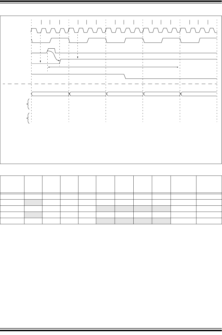
FIGURE 14-8: INT PIN INTERRUPT TIMING
TABLE 14-6: SUMMARY OF INTERRUPT REGISTERS
Name Bit 7 Bit 6 Bit 5 Bit 4 Bit 3 Bit 2 Bit 1 Bit 0
Value on
POR, BOR
Value on
all other
Resets
INTCON GIE PEIE T0IE INTE RABIE T0IF INTF RABIF 0000 000x 0000 000x
PIE1
— ADIE RCIE TXIE SSPIE CCP1IE TMR2IE TMR1IE -000 0000 -000 0000
PIE2 OSFIE C2IE C1IE EEIE
— — — — 0000 ---- 0000 ----
PIR1
— ADIF RCIF TXIF SSPIF CCP1IF TMR2IF TMR1IF -000 0000 -000 0000
PIR2
OSFIF C2IF C1IF EEIF — — — — 0000 ---- 0000 ----
Legend: x = unknown, u = unchanged, — = unimplemented read as ‘0’, q = value depends upon condition.
Shaded cells are not used by the Interrupt module.
Q2Q1 Q3 Q4 Q2Q1 Q3 Q4 Q2Q1 Q3 Q4 Q2Q1 Q3 Q4 Q2Q1 Q3 Q4
OSC1
CLKOUT
INT pin
INTF flag
(INTCON<1>)
GIE bit
(INTCON<7>)
INSTRUCTION FLOW
PC
Instruction
Fetched
Instruction
Executed
Interrupt Latency
PC PC + 1
PC + 1
0004h
0005h
Inst (0004h)
Inst (0005h)
Dummy Cycle
Inst (PC)
Inst (PC + 1)
Inst (PC – 1)
Inst (0004h)
Dummy Cycle
Inst (PC)
—
Note 1: INTF flag is sampled here (every Q1).
2: Asynchronous interrupt latency = 3-4 T
CY. Synchronous latency = 3 TCY, where TCY = instruction cycle time. Latency
is the same whether Inst (PC) is a single cycle or a 2-cycle instruction.
3: CLKOUT is available only in INTOSC and RC Oscillator modes.
4: For minimum width of INT pulse, refer to AC specifications in Section 17.0 “Electrical Specifications”.
5: INTF is enabled to be set any time during the Q4-Q1 cycles.
(1)
(2)
(3)
(4)
(5)
(1)