
Datasheet


© 2007 Microchip Technology Inc. DS41232D-page 105
PIC12F635/PIC16F636/639
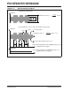
TABLE 11-1: TYPICAL OUTPUT ENABLE
FILTER TIMING
TOEH is measured from the rising edge of the demodulator
output to the first falling edge. The pulse width must fall
within TOEH ≤ t ≤ TOET.
T
OEL is measured from the falling edge of the
demodulator output to the rising edge of the next pulse.
The pulse width must fall within TOEL ≤ t ≤ TOET.
T
OET is measured from rising edge to the next rising
edge (i.e., the sum of T
OEH and TOEL). The pulse width
must be t ≤ T
OET. If the Configuration Register 0
(Register 11-1), OEL<8:7> is set to ‘00’, then T
OEH
must not exceed TOET and TOEL must not exceed
T
INACT.
The filter will reset, requiring a complete new successive
high and low period to enable LFDATA, under the
following conditions.
• The received high is not greater than the
configured minimum T
OEH value.
•During TOEH, a loss of signal > 56 μs. A loss of
signal < 56 μs may or may not cause a filter
Reset.
• The received low is not greater than the
configured minimum T
OEL value.
• The received sequence exceeds the maximum
T
OET value:
-T
OEH + TOEL > TOET
-or TOEH > TOET
-or TOEL > TOET
• A Soft Reset SPI command is received.
If the filter resets due to a long high (T
OEH > TOET), the
high-pulse timer will not begin timing again until after a
gap of TE and another low-to-high transition occurs on
the demodulator output.
Disabling the output enable filter disables the T
OEH and
T
OEL requirement and the AFE passes all received LF
data. See Figure 11-10, Figure 11-11 and Figure 11-12
for examples.
When viewed from an application perspective, from the
pin input, the actual output enable filter timing must fac-
tor in the analog delays in the input path (such as
demodulator charge and discharge times).
• T
OEH - TDR + TDF
• TOEL + TDR - TDF
The output enable filter starts immediately after TGAP,
the gap after AGC stabilization period.
11.16 Input Sensitivity Control
The AFE is designed to have typical input sensitivity of
3mV
PP. This means any input signal with amplitude
greater than 3 mV
PP can be detected. The AFE’s internal
AGC loop regulates the detecting signal amplitude when
the input level is greater than approximately 20 mV
PP.
This signal amplitude is called “AGC-active level”. The
AGC loop regulates the input voltage so that the input
signal amplitude range will be kept within the linear range
of the detection circuits without saturation. The AGC
Active Status bit AGCACT<5>, in the AFE Status
Register 7 (Register 11-8) is set if the AGC loop
regulates the input voltage.
Table 11-2 shows the input sensitivity comparison when
the AGCSIG option is used. When AGCSIG option bit is
set, the demodulated output is available only when the
AGC loop is active (see Table 11-1). The AFE has also
input sensitivity reduction options per each channel. The
Configuration Register 3 (Register 11-4), Configuration
Register 4 (Register 11-5) and Configuration Register 5
(Register 11-6) have the option to reduce the channel
gains from 0 dB to approximately -30 dB.
OEH
<1:0>
OEL
<1:0>
T
OEH
(ms)
T
OEL
(ms)
T
OET
(ms)
01 00 113
01 01 113
01 10 124
01 11 146
10 00 214
10 01 214
10 10 225
10 11 248
11 00 416
11 01 416
11 10 428
11 11 4410
00
XX Filter Disabled
Note 1: Typical at room temperature and
V
DD = 3.0V, 32 kHz oscillator.