
Datasheet


Table Of Contents
- High Performance RISC CPU:
- Special Microcontroller Features:
- Low Power Features:
- Peripheral Features:
- Pin Diagrams
- Most Current Data Sheet
- Errata
- Customer Notification System
- 1.0 General Description
- 2.0 PIC16F627A/628A/648A Device Varieties
- 3.0 Architectural Overview
- 4.0 Memory Organization
- FIGURE 4-1: Program Memory Map and Stack
- TABLE 4-1: general purpose STATIC ram Registers
- TABLE 4-2: Access to Banks of Registers
- FIGURE 4-2: Data Memory Map of the PIC16F627A and PIC16F628A
- FIGURE 4-3: Data Memory Map of the PIC16F648A
- TABLE 4-3: Special Registers Summary Bank0
- TABLE 4-4: Special Function Registers Summary Bank1
- TABLE 4-5: Special Function Registers Summary Bank2
- TABLE 4-6: Special Function Registers Summary Bank3
- FIGURE 4-4: Loading Of PC In Different Situations
- FIGURE 4-5: Direct/Indirect Addressing PIC16F627A/628A/648A
- 5.0 I/O Ports
- FIGURE 5-1: Block Diagram of RA0/AN0:RA1/AN1 Pins
- FIGURE 5-2: Block Diagram of RA2/Vref Pin
- FIGURE 5-3: Block Diagram of the RA3/AN3 Pin
- FIGURE 5-4: Block Diagram of RA4/T0CKI Pin
- FIGURE 5-5: Block Diagram of the RA5/MCLR/Vpp Pin
- FIGURE 5-6: Block Diagram of RA6/OSC2/CLKOUT Pin
- FIGURE 5-7: Block Diagram of RA7/OSC1/CLKIN Pin
- TABLE 5-1: PORTA Functions
- TABLE 5-2: Summary of Registers Associated with PORTA(1)
- FIGURE 5-8: Block Diagram of RB0/INT Pin
- FIGURE 5-9: Block Diagram of RB1/RX/DT Pin
- FIGURE 5-10: Block Diagram of RB2/TX/CK Pin
- FIGURE 5-11: Block Diagram of RB3/CCP1 Pin
- FIGURE 5-12: Block Diagram of RB4/PGM Pin
- FIGURE 5-13: Block Diagram of RB5 Pin
- FIGURE 5-14: Block Diagram of RB6/T1OSO/T1CKI Pin
- FIGURE 5-15: Block Diagram of the RB7/T1OSI Pin
- TABLE 5-3: PORTB Functions
- TABLE 5-4: Summary of Registers Associated With PORTB(1)
- FIGURE 5-16: Successive I/O Operation
- 6.0 Timer0 Module
- 7.0 Timer1 Module
- 8.0 Timer2 Module
- 9.0 Capture/Compare/PWM (CCP) Module
- TABLE 9-1: CCP Mode - Timer Resource
- FIGURE 9-1: Capture Mode Operation Block Diagram
- FIGURE 9-2: Compare Mode Operation Block Diagram
- TABLE 9-2: Registers Associated with Capture, compare, and Timer1
- FIGURE 9-3: Simplified PWM Block Diagram
- FIGURE 9-4: PWM OUTPUT
- TABLE 9-3: Example PWM Frequencies and Resolutions at 20 MHz
- TABLE 9-4: Registers Associated with PWM and Timer2
- 10.0 Comparator Module
- 11.0 Voltage Reference Module
- 12.0 Universal Synchronous Asynchronous Receiver Transmitter (USART) Module
- TABLE 12-1: BAUD rATE fORMULA
- TABLE 12-2: Registers Associated with Baud Rate Generator
- TABLE 12-3: Baud Rates for synchronous Mode
- TABLE 12-4: Baud Rates for Asynchronous Mode (BRGH = 0)
- TABLE 12-5: Baud Rates for Asynchronous Mode (BRGH = 1)
- FIGURE 12-1: RX Pin Sampling Scheme. BRGH = 0
- FIGURE 12-2: RX Pin Sampling Scheme, BRGH = 1
- FIGURE 12-3: RX Pin Sampling Scheme, BRGH = 1
- FIGURE 12-4: RX Pin Sampling Scheme, BRGH = 0 OR BRGH = 1
- FIGURE 12-5: USART Transmit Block Diagram
- FIGURE 12-6: Asynchronous Transmission
- FIGURE 12-7: Asynchronous Transmission (Back to Back)
- TABLE 12-6: Registers Associated with Asynchronous Transmission
- FIGURE 12-8: USART Receive Block Diagram
- FIGURE 12-9: Asynchronous Reception with Address Detect
- FIGURE 12-10: Asynchronous Reception with Address Byte First
- FIGURE 12-11: Asynchronous Reception with Address Byte First Followed by Valid Data Byte
- TABLE 12-7: Registers Associated with Asynchronous Reception
- TABLE 12-8: Registers Associated with Asynchronous Reception
- TABLE 12-9: Registers Associated with Synchronous Master Transmission
- FIGURE 12-12: Synchronous Transmission
- FIGURE 12-13: Synchronous Transmission (Through TXEN)
- TABLE 12-10: Registers Associated with Synchronous Master Reception
- FIGURE 12-14: Synchronous Reception (Master Mode, SREN)
- TABLE 12-11: Registers Associated with Synchronous Slave Transmission
- TABLE 12-12: Registers Associated with Synchronous Slave Reception
- 13.0 Data EEPROM Memory
- 14.0 Special Features of the CPU
- FIGURE 14-1: Crystal Operation (or Ceramic Resonator) (HS, XT or LP Osc Configuration)
- TABLE 14-1: Capacitor Selection for Ceramic Resonators
- TABLE 14-2: Capacitor Selection for Crystal Oscillator
- FIGURE 14-2: External Parallel Resonant Crystal Oscillator Circuit
- FIGURE 14-3: External Series Resonant Crystal Oscillator Circuit
- FIGURE 14-4: External Clock Input Operation (EC, HS, XT or LP Osc Configuration)
- FIGURE 14-5: RC OSCILLATOR MODE
- FIGURE 14-6: Simplified Block Diagram of On-chip Reset Circuit
- FIGURE 14-7: Brown-out Situations WITH PWRT ENABLED
- TABLE 14-3: Time out in Various Situations
- TABLE 14-4: Status/PCON Bits and Their Significance
- TABLE 14-5: Summary of Registers Associated with Brown-out Reset
- TABLE 14-6: Initialization Condition for Special Registers
- TABLE 14-7: Initialization Condition for Registers
- FIGURE 14-8: Time out Sequence on Power-up (MCLR not tied to Vdd): Case
- FIGURE 14-9: Time out Sequence on Power-up (MCLR not tied to Vdd): Case 2
- FIGURE 14-10: Time out Sequence on Power-up (MCLR tied to Vdd)
- FIGURE 14-11: External Power-on Reset Circuit (For Slow Vdd Power-up)
- FIGURE 14-12: External Brown-out Protection Circuit 1
- FIGURE 14-13: External Brown-out Protection Circuit 2
- FIGURE 14-14: Interrupt Logic
- FIGURE 14-15: INT Pin Interrupt Timing
- TABLE 14-8: Summary of interrupt registers
- FIGURE 14-16: Watchdog Timer Block Diagram
- TABLE 14-9: Summary of Watchdog Timer Registers
- FIGURE 14-17: Wake-up from Sleep Through Interrupt
- FIGURE 14-18: Typical In-Circuit Serial Programming Connection
- 15.0 Instruction Set Summary
- 16.0 Development Support
- 17.0 Electrical Specifications
- FIGURE 17-1: PIC16F627A/628A/648A VOLTAGE-FREQUENCY GRAPH, -40°C £ TA £ +125°C
- FIGURE 17-2: PIC16LF627A/628A/648A VOLTAGE-FREQUENCY GRAPH, -40°C £ TA £ +85°C
- TABLE 17-1: DC Characteristics: PIC16F627A/628A/648A (Industrial, Extended) PIC16LF627A/628A/648A...
- TABLE 17-2: Comparator Specifications
- TABLE 17-3: Voltage Reference Specifications
- FIGURE 17-3: Load Conditions
- FIGURE 17-4: External Clock Timing
- TABLE 17-4: External Clock Timing Requirements
- TABLE 17-5: pRECISION INTERNAL OSCILLATOR Parameters
- FIGURE 17-5: CLKOUT and I/O Timing
- TABLE 17-6: CLKOUT and I/O Timing Requirements
- FIGURE 17-6: Reset, Watchdog Timer, Oscillator Start-Up Timer and Power-Up Timer Timing
- FIGURE 17-7: Brown-out Detect Timing
- TABLE 17-7: Reset, Watchdog Timer, Oscillator Start-up Timer and Power-up Timer Requirements
- FIGURE 17-8: Timer0 and Timer1 External Clock Timings
- TABLE 17-9: Timer0 and Timer1 External Clock Requirements
- FIGURE 17-10: Capture/Compare/PWM Timings
- TABLE 17-8: Capture/Compare/PWM Requirements
- FIGURE 17-11: TIMER0 Clock Timing
- TABLE 17-9: TIMER0 Clock Requirements
- 18.0 DC and AC Characteristics Graphs and Tables
- 19.0 Packaging Information
- Appendix A: Data Sheet Revision History
- Appendix B: Device Differences
- Appendix C: Device Migrations
- Appendix D: Migrating from other PICmicro Devices
- Appendix E: Development Tool Version Requirements
- Index
- Product ID System
- Worldwide Sales
2002 Microchip Technology Inc. Preliminary DS40044A-page 97
PIC16F627A/628A/648A
14.2.8 SPECIAL FEATURE: DUAL SPEED
OSCILLATOR MODES
A software programmable dual speed Oscillator mode
is provided when the PIC16F627A/628A/648A is con-
figured in the INTOSC Oscillator mode. This feature
allows users to dynamically toggle the oscillator speed
between 4 MHz and 37 kHz nominal in the INTOSC
mode. Applications that require low current power sav-
ings, but cannot tolerate putting the part into SLEEP,
may use this mode.
There is a time delay associated with the transition
between Fast and Slow oscillator speeds. This Oscilla-
tor Speed Transition delay consists of two existing
clock pulses and eight new speed clock pulses. During
this Clock Speed Transition Delay the System Clock is
halted causing the processor to be frozen in time. Dur-
ing this delay the Program Counter and the Clock Out
stop.
The OSCF bit in the PCON register is used to control
Dual Speed mode. See Section 4.2.2.6, Register 4-6.
14.3 RESET
The PIC16F627A/628A/648A differentiates between
various kinds of RESET:
a) Power-on Reset (POR)
b) MCLR
Reset during normal operation
c) MCLR
Reset during SLEEP
d) WDT Reset (normal operation)
e) WDT wake-up (SLEEP)
f) Brown-out Reset (BOR)
Some registers are not affected in any RESET condi-
tion; their status is unknown on POR and unchanged in
any other RESET. Most other registers are reset to a
“RESET state” on Power-on Reset, Brown-out Reset,
MCLR
Reset, WDT Reset and MCLR Reset during
SLEEP. They are not affected by a WDT wake-up,
since this is viewed as the resumption of normal oper-
ation. TO
and PD bits are set or cleared differently in
different RESET situations as indicated in Table 14-4.
These bits are used in software to determine the nature
of the RESET. See Table 14-7 for a full description of
RESET states of all registers.
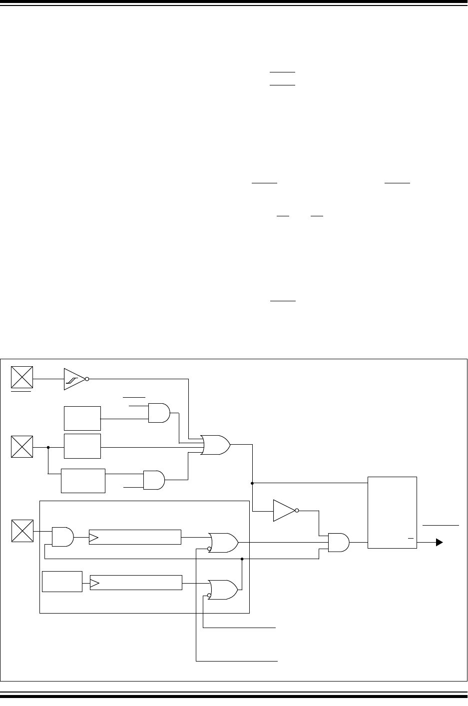
A simplified block diagram of the on-chip RESET circuit
is shown in Figure 14-6.
The MCLR
Reset path has a noise filter to detect and
ignore small pulses. See Table 17-7 for pulse width
specification.
FIGURE 14-6: SIMPLIFIED BLOCK DIAGRAM OF ON-CHIP RESET CIRCUIT
S
R
Q
External
RESET
MCLR/
V
DD
OSC1/
WDT
Module
V
DD rise
detect
OST/PWRT
WDT
Time out
Power-on Reset
OST
PWRT
Chip_Reset
10-bit Ripple-counter
Reset
Enable OST
Enable PWRT
SLEEP
See Table 14-3 for time out situations.
Note 1: This is a separate oscillator from the INTOSC/RC oscillator.
Brown-out
detect Reset
BOREN
CLKIN
Pin
V
PP Pin
10-bit Ripple-counter
Q
Schmitt Trigger Input
On-chip
(1)
OSC