
Datasheet


Table Of Contents
- High Performance RISC CPU:
- Special Microcontroller Features:
- Low Power Features:
- Peripheral Features:
- Pin Diagrams
- Most Current Data Sheet
- Errata
- Customer Notification System
- 1.0 General Description
- 2.0 PIC16F627A/628A/648A Device Varieties
- 3.0 Architectural Overview
- 4.0 Memory Organization
- FIGURE 4-1: Program Memory Map and Stack
- TABLE 4-1: general purpose STATIC ram Registers
- TABLE 4-2: Access to Banks of Registers
- FIGURE 4-2: Data Memory Map of the PIC16F627A and PIC16F628A
- FIGURE 4-3: Data Memory Map of the PIC16F648A
- TABLE 4-3: Special Registers Summary Bank0
- TABLE 4-4: Special Function Registers Summary Bank1
- TABLE 4-5: Special Function Registers Summary Bank2
- TABLE 4-6: Special Function Registers Summary Bank3
- FIGURE 4-4: Loading Of PC In Different Situations
- FIGURE 4-5: Direct/Indirect Addressing PIC16F627A/628A/648A
- 5.0 I/O Ports
- FIGURE 5-1: Block Diagram of RA0/AN0:RA1/AN1 Pins
- FIGURE 5-2: Block Diagram of RA2/Vref Pin
- FIGURE 5-3: Block Diagram of the RA3/AN3 Pin
- FIGURE 5-4: Block Diagram of RA4/T0CKI Pin
- FIGURE 5-5: Block Diagram of the RA5/MCLR/Vpp Pin
- FIGURE 5-6: Block Diagram of RA6/OSC2/CLKOUT Pin
- FIGURE 5-7: Block Diagram of RA7/OSC1/CLKIN Pin
- TABLE 5-1: PORTA Functions
- TABLE 5-2: Summary of Registers Associated with PORTA(1)
- FIGURE 5-8: Block Diagram of RB0/INT Pin
- FIGURE 5-9: Block Diagram of RB1/RX/DT Pin
- FIGURE 5-10: Block Diagram of RB2/TX/CK Pin
- FIGURE 5-11: Block Diagram of RB3/CCP1 Pin
- FIGURE 5-12: Block Diagram of RB4/PGM Pin
- FIGURE 5-13: Block Diagram of RB5 Pin
- FIGURE 5-14: Block Diagram of RB6/T1OSO/T1CKI Pin
- FIGURE 5-15: Block Diagram of the RB7/T1OSI Pin
- TABLE 5-3: PORTB Functions
- TABLE 5-4: Summary of Registers Associated With PORTB(1)
- FIGURE 5-16: Successive I/O Operation
- 6.0 Timer0 Module
- 7.0 Timer1 Module
- 8.0 Timer2 Module
- 9.0 Capture/Compare/PWM (CCP) Module
- TABLE 9-1: CCP Mode - Timer Resource
- FIGURE 9-1: Capture Mode Operation Block Diagram
- FIGURE 9-2: Compare Mode Operation Block Diagram
- TABLE 9-2: Registers Associated with Capture, compare, and Timer1
- FIGURE 9-3: Simplified PWM Block Diagram
- FIGURE 9-4: PWM OUTPUT
- TABLE 9-3: Example PWM Frequencies and Resolutions at 20 MHz
- TABLE 9-4: Registers Associated with PWM and Timer2
- 10.0 Comparator Module
- 11.0 Voltage Reference Module
- 12.0 Universal Synchronous Asynchronous Receiver Transmitter (USART) Module
- TABLE 12-1: BAUD rATE fORMULA
- TABLE 12-2: Registers Associated with Baud Rate Generator
- TABLE 12-3: Baud Rates for synchronous Mode
- TABLE 12-4: Baud Rates for Asynchronous Mode (BRGH = 0)
- TABLE 12-5: Baud Rates for Asynchronous Mode (BRGH = 1)
- FIGURE 12-1: RX Pin Sampling Scheme. BRGH = 0
- FIGURE 12-2: RX Pin Sampling Scheme, BRGH = 1
- FIGURE 12-3: RX Pin Sampling Scheme, BRGH = 1
- FIGURE 12-4: RX Pin Sampling Scheme, BRGH = 0 OR BRGH = 1
- FIGURE 12-5: USART Transmit Block Diagram
- FIGURE 12-6: Asynchronous Transmission
- FIGURE 12-7: Asynchronous Transmission (Back to Back)
- TABLE 12-6: Registers Associated with Asynchronous Transmission
- FIGURE 12-8: USART Receive Block Diagram
- FIGURE 12-9: Asynchronous Reception with Address Detect
- FIGURE 12-10: Asynchronous Reception with Address Byte First
- FIGURE 12-11: Asynchronous Reception with Address Byte First Followed by Valid Data Byte
- TABLE 12-7: Registers Associated with Asynchronous Reception
- TABLE 12-8: Registers Associated with Asynchronous Reception
- TABLE 12-9: Registers Associated with Synchronous Master Transmission
- FIGURE 12-12: Synchronous Transmission
- FIGURE 12-13: Synchronous Transmission (Through TXEN)
- TABLE 12-10: Registers Associated with Synchronous Master Reception
- FIGURE 12-14: Synchronous Reception (Master Mode, SREN)
- TABLE 12-11: Registers Associated with Synchronous Slave Transmission
- TABLE 12-12: Registers Associated with Synchronous Slave Reception
- 13.0 Data EEPROM Memory
- 14.0 Special Features of the CPU
- FIGURE 14-1: Crystal Operation (or Ceramic Resonator) (HS, XT or LP Osc Configuration)
- TABLE 14-1: Capacitor Selection for Ceramic Resonators
- TABLE 14-2: Capacitor Selection for Crystal Oscillator
- FIGURE 14-2: External Parallel Resonant Crystal Oscillator Circuit
- FIGURE 14-3: External Series Resonant Crystal Oscillator Circuit
- FIGURE 14-4: External Clock Input Operation (EC, HS, XT or LP Osc Configuration)
- FIGURE 14-5: RC OSCILLATOR MODE
- FIGURE 14-6: Simplified Block Diagram of On-chip Reset Circuit
- FIGURE 14-7: Brown-out Situations WITH PWRT ENABLED
- TABLE 14-3: Time out in Various Situations
- TABLE 14-4: Status/PCON Bits and Their Significance
- TABLE 14-5: Summary of Registers Associated with Brown-out Reset
- TABLE 14-6: Initialization Condition for Special Registers
- TABLE 14-7: Initialization Condition for Registers
- FIGURE 14-8: Time out Sequence on Power-up (MCLR not tied to Vdd): Case
- FIGURE 14-9: Time out Sequence on Power-up (MCLR not tied to Vdd): Case 2
- FIGURE 14-10: Time out Sequence on Power-up (MCLR tied to Vdd)
- FIGURE 14-11: External Power-on Reset Circuit (For Slow Vdd Power-up)
- FIGURE 14-12: External Brown-out Protection Circuit 1
- FIGURE 14-13: External Brown-out Protection Circuit 2
- FIGURE 14-14: Interrupt Logic
- FIGURE 14-15: INT Pin Interrupt Timing
- TABLE 14-8: Summary of interrupt registers
- FIGURE 14-16: Watchdog Timer Block Diagram
- TABLE 14-9: Summary of Watchdog Timer Registers
- FIGURE 14-17: Wake-up from Sleep Through Interrupt
- FIGURE 14-18: Typical In-Circuit Serial Programming Connection
- 15.0 Instruction Set Summary
- 16.0 Development Support
- 17.0 Electrical Specifications
- FIGURE 17-1: PIC16F627A/628A/648A VOLTAGE-FREQUENCY GRAPH, -40°C £ TA £ +125°C
- FIGURE 17-2: PIC16LF627A/628A/648A VOLTAGE-FREQUENCY GRAPH, -40°C £ TA £ +85°C
- TABLE 17-1: DC Characteristics: PIC16F627A/628A/648A (Industrial, Extended) PIC16LF627A/628A/648A...
- TABLE 17-2: Comparator Specifications
- TABLE 17-3: Voltage Reference Specifications
- FIGURE 17-3: Load Conditions
- FIGURE 17-4: External Clock Timing
- TABLE 17-4: External Clock Timing Requirements
- TABLE 17-5: pRECISION INTERNAL OSCILLATOR Parameters
- FIGURE 17-5: CLKOUT and I/O Timing
- TABLE 17-6: CLKOUT and I/O Timing Requirements
- FIGURE 17-6: Reset, Watchdog Timer, Oscillator Start-Up Timer and Power-Up Timer Timing
- FIGURE 17-7: Brown-out Detect Timing
- TABLE 17-7: Reset, Watchdog Timer, Oscillator Start-up Timer and Power-up Timer Requirements
- FIGURE 17-8: Timer0 and Timer1 External Clock Timings
- TABLE 17-9: Timer0 and Timer1 External Clock Requirements
- FIGURE 17-10: Capture/Compare/PWM Timings
- TABLE 17-8: Capture/Compare/PWM Requirements
- FIGURE 17-11: TIMER0 Clock Timing
- TABLE 17-9: TIMER0 Clock Requirements
- 18.0 DC and AC Characteristics Graphs and Tables
- 19.0 Packaging Information
- Appendix A: Data Sheet Revision History
- Appendix B: Device Differences
- Appendix C: Device Migrations
- Appendix D: Migrating from other PICmicro Devices
- Appendix E: Development Tool Version Requirements
- Index
- Product ID System
- Worldwide Sales
2002 Microchip Technology Inc. Preliminary DS40044A-page 95
PIC16F627A/628A/648A
14.2 Oscillator Configurations
14.2.1 OSCILLATOR TYPES
The PIC16F627A/628A/648A can be operated in eight
different oscillator options. The user can program three
configuration bits (FOSC2 through FOSC0) to select
one of these eight modes:
• LP Low Power Crystal
• XT Crystal/Resonator
• HS High Speed Crystal/Resonator
• RC External Resistor/Capacitor (2 modes)
• INTOSC Internal Precision Oscillator (2 modes)
• EC External Clock In
14.2.2 CRYSTAL OSCILLATOR / CERAMIC
RESONATORS
In XT, LP or HS modes a crystal or ceramic resonator
is connected to the OSC1 and OSC2 pins to establish
oscillation (Figure 14-1). The PIC16F627A/628A/648A
oscillator design requires the use of a parallel cut crys-
tal. Use of a series cut crystal may give a frequency out
of the crystal manufacturers specifications. When in
XT, LP or HS modes, the device can have an external
clock source to drive the OSC1 pin (Figure 14-4).
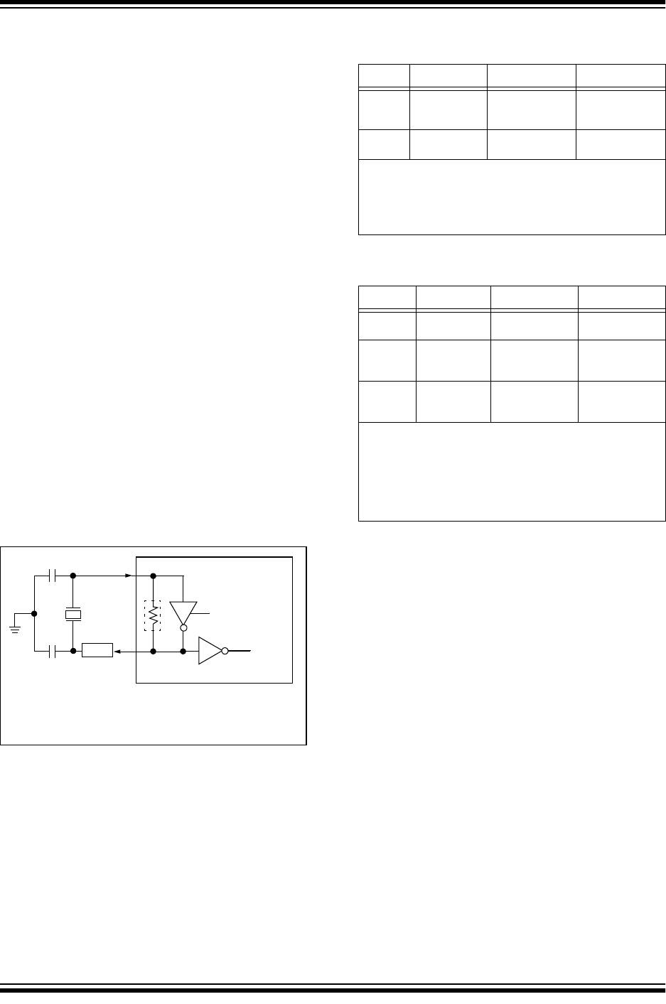
FIGURE 14-1: CRYSTAL OPERATION
(OR CERAMIC
RESONATOR) (HS, XT OR
LP OSC
CONFIGURATION)
TABLE 14-1: CAPACITOR SELECTION FOR
CERAMIC RESONATORS
TABLE 14-2: CAPACITOR SELECTION FOR
CRYSTAL OSCILLATOR
14.2.3 EXTERNAL CRYSTAL OSCILLATOR
CIRCUIT
Either a prepackaged oscillator can be used or a simple
oscillator circuit with TTL gates can be built.
Prepackaged oscillators provide a wide operating
range and better stability. A well-designed crystal
oscillator will provide good performance with TTL
gates. Two types of crystal oscillator circuits can be
used; one with series resonance, or one with parallel
resonance.
Figure 14-2 shows implementation of a parallel reso-
nant oscillator circuit. The circuit is designed to use the
fundamental frequency of the crystal. The 74AS04
inverter performs the 180° phase shift that a parallel
oscillator requires. The 4.7 kΩ resistor provides the
negative feedback for stability. The 10 kΩ
potentiometers bias the 74AS04 in the linear region.
This could be used for external oscillator designs.
Note 1: A series resistor may be required for AT strip cut
crystals.
2: See Table 14-1 and Table 14-2 for recommended
values of C1 and C2.
C1
C2
XTAL
OSC2
RS
(1)
OSC1
RF
SLEEP
PIC16F627A/628A/648A
FOSC
Mode Freq OSC1(C1) OSC2(C2)
XT 455 kHz
2.0 MHz
4.0 MHz
22 - 100 pF
15 - 68 pF
15 - 68 pF
22 - 100 pF
15 - 68 pF
15 - 68 pF
HS 8.0 MHz
16.0 MHz
10 - 68 pF
10 - 22 pF
10 - 68 pF
10 - 22 pF
Note: Higher capacitance increases the stability of the oscil-
lator but also increases the start-up time. These values
are for design guidance only. Since each resonator has
its own characteristics, the user should consult the res-
onator manufacturer for appropriate values of external
components.
Mode Freq OSC1(C1) OSC2(C2)
LP 32 kHz
200 kHz
15 - 30 pF
0 - 15 pF
15 - 30 pF
0 - 15 pF
XT 100 kHz
2 MHz
4 MHz
68 - 150 pF
15 - 30 pF
15 - 30 pF
150 - 200 pF
15 - 30 pF
15 - 30 pF
HS 8 MHz
10 MHz
20 MHz
15 - 30 pF
15 - 30 pF
15 - 30 pF
15 - 30 pF
15 - 30 pF
15 - 30 pF
Note: Higher capacitance increases the stability of the oscil-
lator but also increases the start-up time. These values
are for design guidance only. A series resistor (RS)
may be required in HS mode as well as XT mode to
avoid overdriving crystals with low drive level specifica-
tion. Since each crystal has its own characteristics, the
user should consult the crystal manufacturer for appro-
priate values of external components.