
Datasheet


Table Of Contents
- High Performance RISC CPU:
- Special Microcontroller Features:
- Low Power Features:
- Peripheral Features:
- Pin Diagrams
- Most Current Data Sheet
- Errata
- Customer Notification System
- 1.0 General Description
- 2.0 PIC16F627A/628A/648A Device Varieties
- 3.0 Architectural Overview
- 4.0 Memory Organization
- FIGURE 4-1: Program Memory Map and Stack
- TABLE 4-1: general purpose STATIC ram Registers
- TABLE 4-2: Access to Banks of Registers
- FIGURE 4-2: Data Memory Map of the PIC16F627A and PIC16F628A
- FIGURE 4-3: Data Memory Map of the PIC16F648A
- TABLE 4-3: Special Registers Summary Bank0
- TABLE 4-4: Special Function Registers Summary Bank1
- TABLE 4-5: Special Function Registers Summary Bank2
- TABLE 4-6: Special Function Registers Summary Bank3
- FIGURE 4-4: Loading Of PC In Different Situations
- FIGURE 4-5: Direct/Indirect Addressing PIC16F627A/628A/648A
- 5.0 I/O Ports
- FIGURE 5-1: Block Diagram of RA0/AN0:RA1/AN1 Pins
- FIGURE 5-2: Block Diagram of RA2/Vref Pin
- FIGURE 5-3: Block Diagram of the RA3/AN3 Pin
- FIGURE 5-4: Block Diagram of RA4/T0CKI Pin
- FIGURE 5-5: Block Diagram of the RA5/MCLR/Vpp Pin
- FIGURE 5-6: Block Diagram of RA6/OSC2/CLKOUT Pin
- FIGURE 5-7: Block Diagram of RA7/OSC1/CLKIN Pin
- TABLE 5-1: PORTA Functions
- TABLE 5-2: Summary of Registers Associated with PORTA(1)
- FIGURE 5-8: Block Diagram of RB0/INT Pin
- FIGURE 5-9: Block Diagram of RB1/RX/DT Pin
- FIGURE 5-10: Block Diagram of RB2/TX/CK Pin
- FIGURE 5-11: Block Diagram of RB3/CCP1 Pin
- FIGURE 5-12: Block Diagram of RB4/PGM Pin
- FIGURE 5-13: Block Diagram of RB5 Pin
- FIGURE 5-14: Block Diagram of RB6/T1OSO/T1CKI Pin
- FIGURE 5-15: Block Diagram of the RB7/T1OSI Pin
- TABLE 5-3: PORTB Functions
- TABLE 5-4: Summary of Registers Associated With PORTB(1)
- FIGURE 5-16: Successive I/O Operation
- 6.0 Timer0 Module
- 7.0 Timer1 Module
- 8.0 Timer2 Module
- 9.0 Capture/Compare/PWM (CCP) Module
- TABLE 9-1: CCP Mode - Timer Resource
- FIGURE 9-1: Capture Mode Operation Block Diagram
- FIGURE 9-2: Compare Mode Operation Block Diagram
- TABLE 9-2: Registers Associated with Capture, compare, and Timer1
- FIGURE 9-3: Simplified PWM Block Diagram
- FIGURE 9-4: PWM OUTPUT
- TABLE 9-3: Example PWM Frequencies and Resolutions at 20 MHz
- TABLE 9-4: Registers Associated with PWM and Timer2
- 10.0 Comparator Module
- 11.0 Voltage Reference Module
- 12.0 Universal Synchronous Asynchronous Receiver Transmitter (USART) Module
- TABLE 12-1: BAUD rATE fORMULA
- TABLE 12-2: Registers Associated with Baud Rate Generator
- TABLE 12-3: Baud Rates for synchronous Mode
- TABLE 12-4: Baud Rates for Asynchronous Mode (BRGH = 0)
- TABLE 12-5: Baud Rates for Asynchronous Mode (BRGH = 1)
- FIGURE 12-1: RX Pin Sampling Scheme. BRGH = 0
- FIGURE 12-2: RX Pin Sampling Scheme, BRGH = 1
- FIGURE 12-3: RX Pin Sampling Scheme, BRGH = 1
- FIGURE 12-4: RX Pin Sampling Scheme, BRGH = 0 OR BRGH = 1
- FIGURE 12-5: USART Transmit Block Diagram
- FIGURE 12-6: Asynchronous Transmission
- FIGURE 12-7: Asynchronous Transmission (Back to Back)
- TABLE 12-6: Registers Associated with Asynchronous Transmission
- FIGURE 12-8: USART Receive Block Diagram
- FIGURE 12-9: Asynchronous Reception with Address Detect
- FIGURE 12-10: Asynchronous Reception with Address Byte First
- FIGURE 12-11: Asynchronous Reception with Address Byte First Followed by Valid Data Byte
- TABLE 12-7: Registers Associated with Asynchronous Reception
- TABLE 12-8: Registers Associated with Asynchronous Reception
- TABLE 12-9: Registers Associated with Synchronous Master Transmission
- FIGURE 12-12: Synchronous Transmission
- FIGURE 12-13: Synchronous Transmission (Through TXEN)
- TABLE 12-10: Registers Associated with Synchronous Master Reception
- FIGURE 12-14: Synchronous Reception (Master Mode, SREN)
- TABLE 12-11: Registers Associated with Synchronous Slave Transmission
- TABLE 12-12: Registers Associated with Synchronous Slave Reception
- 13.0 Data EEPROM Memory
- 14.0 Special Features of the CPU
- FIGURE 14-1: Crystal Operation (or Ceramic Resonator) (HS, XT or LP Osc Configuration)
- TABLE 14-1: Capacitor Selection for Ceramic Resonators
- TABLE 14-2: Capacitor Selection for Crystal Oscillator
- FIGURE 14-2: External Parallel Resonant Crystal Oscillator Circuit
- FIGURE 14-3: External Series Resonant Crystal Oscillator Circuit
- FIGURE 14-4: External Clock Input Operation (EC, HS, XT or LP Osc Configuration)
- FIGURE 14-5: RC OSCILLATOR MODE
- FIGURE 14-6: Simplified Block Diagram of On-chip Reset Circuit
- FIGURE 14-7: Brown-out Situations WITH PWRT ENABLED
- TABLE 14-3: Time out in Various Situations
- TABLE 14-4: Status/PCON Bits and Their Significance
- TABLE 14-5: Summary of Registers Associated with Brown-out Reset
- TABLE 14-6: Initialization Condition for Special Registers
- TABLE 14-7: Initialization Condition for Registers
- FIGURE 14-8: Time out Sequence on Power-up (MCLR not tied to Vdd): Case
- FIGURE 14-9: Time out Sequence on Power-up (MCLR not tied to Vdd): Case 2
- FIGURE 14-10: Time out Sequence on Power-up (MCLR tied to Vdd)
- FIGURE 14-11: External Power-on Reset Circuit (For Slow Vdd Power-up)
- FIGURE 14-12: External Brown-out Protection Circuit 1
- FIGURE 14-13: External Brown-out Protection Circuit 2
- FIGURE 14-14: Interrupt Logic
- FIGURE 14-15: INT Pin Interrupt Timing
- TABLE 14-8: Summary of interrupt registers
- FIGURE 14-16: Watchdog Timer Block Diagram
- TABLE 14-9: Summary of Watchdog Timer Registers
- FIGURE 14-17: Wake-up from Sleep Through Interrupt
- FIGURE 14-18: Typical In-Circuit Serial Programming Connection
- 15.0 Instruction Set Summary
- 16.0 Development Support
- 17.0 Electrical Specifications
- FIGURE 17-1: PIC16F627A/628A/648A VOLTAGE-FREQUENCY GRAPH, -40°C £ TA £ +125°C
- FIGURE 17-2: PIC16LF627A/628A/648A VOLTAGE-FREQUENCY GRAPH, -40°C £ TA £ +85°C
- TABLE 17-1: DC Characteristics: PIC16F627A/628A/648A (Industrial, Extended) PIC16LF627A/628A/648A...
- TABLE 17-2: Comparator Specifications
- TABLE 17-3: Voltage Reference Specifications
- FIGURE 17-3: Load Conditions
- FIGURE 17-4: External Clock Timing
- TABLE 17-4: External Clock Timing Requirements
- TABLE 17-5: pRECISION INTERNAL OSCILLATOR Parameters
- FIGURE 17-5: CLKOUT and I/O Timing
- TABLE 17-6: CLKOUT and I/O Timing Requirements
- FIGURE 17-6: Reset, Watchdog Timer, Oscillator Start-Up Timer and Power-Up Timer Timing
- FIGURE 17-7: Brown-out Detect Timing
- TABLE 17-7: Reset, Watchdog Timer, Oscillator Start-up Timer and Power-up Timer Requirements
- FIGURE 17-8: Timer0 and Timer1 External Clock Timings
- TABLE 17-9: Timer0 and Timer1 External Clock Requirements
- FIGURE 17-10: Capture/Compare/PWM Timings
- TABLE 17-8: Capture/Compare/PWM Requirements
- FIGURE 17-11: TIMER0 Clock Timing
- TABLE 17-9: TIMER0 Clock Requirements
- 18.0 DC and AC Characteristics Graphs and Tables
- 19.0 Packaging Information
- Appendix A: Data Sheet Revision History
- Appendix B: Device Differences
- Appendix C: Device Migrations
- Appendix D: Migrating from other PICmicro Devices
- Appendix E: Development Tool Version Requirements
- Index
- Product ID System
- Worldwide Sales
PIC16F627A/628A/648A
DS40044A-page 92 Preliminary 2002 Microchip Technology Inc.
13.7 Using the Data EEPROM
The data EEPROM is a high endurance, byte address-
able array that has been optimized for the storage of
frequently changing information (e.g., program vari-
ables or other data that are updated often). Frequently
changing values will typically be updated more often
than specification D124. If this is not the case, an array
refresh must be performed. For this reason, variables
that change infrequently (such as constants, IDs, cali-
bration, etc.) should be stored in FLASH program
memory.
A simple data EEPROM refresh routine is shown in
Example 13-4.
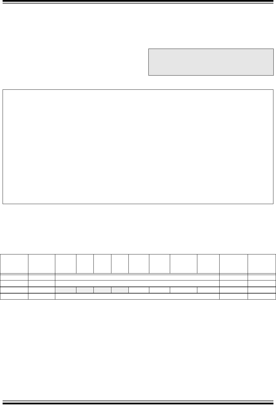
EXAMPLE 13-4: DATA EEPROM REFRESH ROUTINE
13.8 DATA EEPROM OPERATION
DURING CODE PROTECT
When the device is code protected, the CPU is able to
read and write data to the Data EEPROM.
TABLE 13-1: REGISTERS/BITS ASSOCIATED WITH DATA EEPROM
Note: If data EEPROM is only used to store con-
stants and/or data that changes rarely, an
array refresh is likely not required. See
specification D124.
clrf EEADR ; Start at address 0
bcf EECON1,CFGS ; Set for memory
bcf EECON1,EEPGD ; Set for Data EEPROM
bcf INTCON,GIE ; Disable interrupts
bsf EECON1,WREN ; Enable writes
Loop ; Loop to refresh array
bsf EECON1,RD ; Read current address
movlw 55h ;
movwf EECON2 ; Write 55h
movlw AAh ;
movwf EECON2 ; Write AAh
bsf EECON1,WR ; Set WR bit to begin write
btfsc EECON1,WR ; Wait for write to complete
bra $-2
incfsz EEADR,F ; Increment address
bra Loop ; Not zero, do it again
bcf EECON1,WREN ; Disable writes
bsf INTCON,GIE ; Enable interrupts
Address Name Bit 7 Bit 6 Bit 5 Bit 4 Bit 3 Bit 2 Bit 1 Bit 0
Value on
Power-on
Reset
Value on all
other
RESETS
9Ah EEDATA EEPROM data register xxxx xxxx uuuu uuuu
9Bh EEADR EEPROM address register xxxx xxxx uuuu uuuu
9Ch EECON1
— — — — WRERR WREN WR RD ---- x000 ---- q000
9Dh EECON2
(1)
EEPROM control register 2 ---- ---- ---- ----
Legend: x = unknown, u = unchanged, - = unimplemented read as '0', q = value depends upon condition.
Shaded cells are not used by data EEPROM.
Note 1: EECON2 is not a physical register