
Datasheet


Table Of Contents
- High Performance RISC CPU:
- Special Microcontroller Features:
- Low Power Features:
- Peripheral Features:
- Pin Diagrams
- Most Current Data Sheet
- Errata
- Customer Notification System
- 1.0 General Description
- 2.0 PIC16F627A/628A/648A Device Varieties
- 3.0 Architectural Overview
- 4.0 Memory Organization
- FIGURE 4-1: Program Memory Map and Stack
- TABLE 4-1: general purpose STATIC ram Registers
- TABLE 4-2: Access to Banks of Registers
- FIGURE 4-2: Data Memory Map of the PIC16F627A and PIC16F628A
- FIGURE 4-3: Data Memory Map of the PIC16F648A
- TABLE 4-3: Special Registers Summary Bank0
- TABLE 4-4: Special Function Registers Summary Bank1
- TABLE 4-5: Special Function Registers Summary Bank2
- TABLE 4-6: Special Function Registers Summary Bank3
- FIGURE 4-4: Loading Of PC In Different Situations
- FIGURE 4-5: Direct/Indirect Addressing PIC16F627A/628A/648A
- 5.0 I/O Ports
- FIGURE 5-1: Block Diagram of RA0/AN0:RA1/AN1 Pins
- FIGURE 5-2: Block Diagram of RA2/Vref Pin
- FIGURE 5-3: Block Diagram of the RA3/AN3 Pin
- FIGURE 5-4: Block Diagram of RA4/T0CKI Pin
- FIGURE 5-5: Block Diagram of the RA5/MCLR/Vpp Pin
- FIGURE 5-6: Block Diagram of RA6/OSC2/CLKOUT Pin
- FIGURE 5-7: Block Diagram of RA7/OSC1/CLKIN Pin
- TABLE 5-1: PORTA Functions
- TABLE 5-2: Summary of Registers Associated with PORTA(1)
- FIGURE 5-8: Block Diagram of RB0/INT Pin
- FIGURE 5-9: Block Diagram of RB1/RX/DT Pin
- FIGURE 5-10: Block Diagram of RB2/TX/CK Pin
- FIGURE 5-11: Block Diagram of RB3/CCP1 Pin
- FIGURE 5-12: Block Diagram of RB4/PGM Pin
- FIGURE 5-13: Block Diagram of RB5 Pin
- FIGURE 5-14: Block Diagram of RB6/T1OSO/T1CKI Pin
- FIGURE 5-15: Block Diagram of the RB7/T1OSI Pin
- TABLE 5-3: PORTB Functions
- TABLE 5-4: Summary of Registers Associated With PORTB(1)
- FIGURE 5-16: Successive I/O Operation
- 6.0 Timer0 Module
- 7.0 Timer1 Module
- 8.0 Timer2 Module
- 9.0 Capture/Compare/PWM (CCP) Module
- TABLE 9-1: CCP Mode - Timer Resource
- FIGURE 9-1: Capture Mode Operation Block Diagram
- FIGURE 9-2: Compare Mode Operation Block Diagram
- TABLE 9-2: Registers Associated with Capture, compare, and Timer1
- FIGURE 9-3: Simplified PWM Block Diagram
- FIGURE 9-4: PWM OUTPUT
- TABLE 9-3: Example PWM Frequencies and Resolutions at 20 MHz
- TABLE 9-4: Registers Associated with PWM and Timer2
- 10.0 Comparator Module
- 11.0 Voltage Reference Module
- 12.0 Universal Synchronous Asynchronous Receiver Transmitter (USART) Module
- TABLE 12-1: BAUD rATE fORMULA
- TABLE 12-2: Registers Associated with Baud Rate Generator
- TABLE 12-3: Baud Rates for synchronous Mode
- TABLE 12-4: Baud Rates for Asynchronous Mode (BRGH = 0)
- TABLE 12-5: Baud Rates for Asynchronous Mode (BRGH = 1)
- FIGURE 12-1: RX Pin Sampling Scheme. BRGH = 0
- FIGURE 12-2: RX Pin Sampling Scheme, BRGH = 1
- FIGURE 12-3: RX Pin Sampling Scheme, BRGH = 1
- FIGURE 12-4: RX Pin Sampling Scheme, BRGH = 0 OR BRGH = 1
- FIGURE 12-5: USART Transmit Block Diagram
- FIGURE 12-6: Asynchronous Transmission
- FIGURE 12-7: Asynchronous Transmission (Back to Back)
- TABLE 12-6: Registers Associated with Asynchronous Transmission
- FIGURE 12-8: USART Receive Block Diagram
- FIGURE 12-9: Asynchronous Reception with Address Detect
- FIGURE 12-10: Asynchronous Reception with Address Byte First
- FIGURE 12-11: Asynchronous Reception with Address Byte First Followed by Valid Data Byte
- TABLE 12-7: Registers Associated with Asynchronous Reception
- TABLE 12-8: Registers Associated with Asynchronous Reception
- TABLE 12-9: Registers Associated with Synchronous Master Transmission
- FIGURE 12-12: Synchronous Transmission
- FIGURE 12-13: Synchronous Transmission (Through TXEN)
- TABLE 12-10: Registers Associated with Synchronous Master Reception
- FIGURE 12-14: Synchronous Reception (Master Mode, SREN)
- TABLE 12-11: Registers Associated with Synchronous Slave Transmission
- TABLE 12-12: Registers Associated with Synchronous Slave Reception
- 13.0 Data EEPROM Memory
- 14.0 Special Features of the CPU
- FIGURE 14-1: Crystal Operation (or Ceramic Resonator) (HS, XT or LP Osc Configuration)
- TABLE 14-1: Capacitor Selection for Ceramic Resonators
- TABLE 14-2: Capacitor Selection for Crystal Oscillator
- FIGURE 14-2: External Parallel Resonant Crystal Oscillator Circuit
- FIGURE 14-3: External Series Resonant Crystal Oscillator Circuit
- FIGURE 14-4: External Clock Input Operation (EC, HS, XT or LP Osc Configuration)
- FIGURE 14-5: RC OSCILLATOR MODE
- FIGURE 14-6: Simplified Block Diagram of On-chip Reset Circuit
- FIGURE 14-7: Brown-out Situations WITH PWRT ENABLED
- TABLE 14-3: Time out in Various Situations
- TABLE 14-4: Status/PCON Bits and Their Significance
- TABLE 14-5: Summary of Registers Associated with Brown-out Reset
- TABLE 14-6: Initialization Condition for Special Registers
- TABLE 14-7: Initialization Condition for Registers
- FIGURE 14-8: Time out Sequence on Power-up (MCLR not tied to Vdd): Case
- FIGURE 14-9: Time out Sequence on Power-up (MCLR not tied to Vdd): Case 2
- FIGURE 14-10: Time out Sequence on Power-up (MCLR tied to Vdd)
- FIGURE 14-11: External Power-on Reset Circuit (For Slow Vdd Power-up)
- FIGURE 14-12: External Brown-out Protection Circuit 1
- FIGURE 14-13: External Brown-out Protection Circuit 2
- FIGURE 14-14: Interrupt Logic
- FIGURE 14-15: INT Pin Interrupt Timing
- TABLE 14-8: Summary of interrupt registers
- FIGURE 14-16: Watchdog Timer Block Diagram
- TABLE 14-9: Summary of Watchdog Timer Registers
- FIGURE 14-17: Wake-up from Sleep Through Interrupt
- FIGURE 14-18: Typical In-Circuit Serial Programming Connection
- 15.0 Instruction Set Summary
- 16.0 Development Support
- 17.0 Electrical Specifications
- FIGURE 17-1: PIC16F627A/628A/648A VOLTAGE-FREQUENCY GRAPH, -40°C £ TA £ +125°C
- FIGURE 17-2: PIC16LF627A/628A/648A VOLTAGE-FREQUENCY GRAPH, -40°C £ TA £ +85°C
- TABLE 17-1: DC Characteristics: PIC16F627A/628A/648A (Industrial, Extended) PIC16LF627A/628A/648A...
- TABLE 17-2: Comparator Specifications
- TABLE 17-3: Voltage Reference Specifications
- FIGURE 17-3: Load Conditions
- FIGURE 17-4: External Clock Timing
- TABLE 17-4: External Clock Timing Requirements
- TABLE 17-5: pRECISION INTERNAL OSCILLATOR Parameters
- FIGURE 17-5: CLKOUT and I/O Timing
- TABLE 17-6: CLKOUT and I/O Timing Requirements
- FIGURE 17-6: Reset, Watchdog Timer, Oscillator Start-Up Timer and Power-Up Timer Timing
- FIGURE 17-7: Brown-out Detect Timing
- TABLE 17-7: Reset, Watchdog Timer, Oscillator Start-up Timer and Power-up Timer Requirements
- FIGURE 17-8: Timer0 and Timer1 External Clock Timings
- TABLE 17-9: Timer0 and Timer1 External Clock Requirements
- FIGURE 17-10: Capture/Compare/PWM Timings
- TABLE 17-8: Capture/Compare/PWM Requirements
- FIGURE 17-11: TIMER0 Clock Timing
- TABLE 17-9: TIMER0 Clock Requirements
- 18.0 DC and AC Characteristics Graphs and Tables
- 19.0 Packaging Information
- Appendix A: Data Sheet Revision History
- Appendix B: Device Differences
- Appendix C: Device Migrations
- Appendix D: Migrating from other PICmicro Devices
- Appendix E: Development Tool Version Requirements
- Index
- Product ID System
- Worldwide Sales
2002 Microchip Technology Inc. Preliminary DS40044A-page 5
PIC16F627A/628A/648A
1.0 GENERAL DESCRIPTION
The PIC16F627A/628A/648A are 18-Pin FLASH-
based members of the versatile PIC16CXX family of
low cost, high performance, CMOS, fully-static, 8-bit
microcontrollers.
All PICmicro
®
microcontrollers employ an advanced
RISC architecture. The PIC16F627A/628A/648A have
enhanced core features, eight-level deep stack, and
multiple internal and external interrupt sources. The
separate instruction and data buses of the Harvard
architecture allow a 14-bit wide instruction word with
the separate 8-bit wide data. The two-stage instruction
pipeline allows all instructions to execute in a single-
cycle, except for program branches (which require two
cycles). A total of 35 instructions (reduced instruction
set) are available, complemented by a large register
set.
PIC16F627A/628A/648A microcontrollers typically
achieve a 2:1 code compression and a 4:1 speed
improvement over other 8-bit microcontrollers in their
class.
PIC16F627A/628A/648A devices have integrated fea-
tures to reduce external components, thus reducing
system cost, enhancing system reliability and reducing
power consumption.
The PIC16F627A/628A/648A has 8 oscillator configu-
rations. The single-pin RC oscillator provides a low cost
solution. The LP oscillator minimizes power consump-
tion, XT is a standard crystal, and INTOSC is a self-
contained precision two-speed internal oscillator. The
HS is for High-Speed crystals. The EC mode is for an
external clock source.
The SLEEP (Power-down) mode offers power savings.
Users can wake-up the chip from SLEEP through sev-
eral external interrupts, internal interrupts and
RESETS.
A highly reliable Watchdog Timer with its own on-chip
RC oscillator provides protection against software lock-
up.
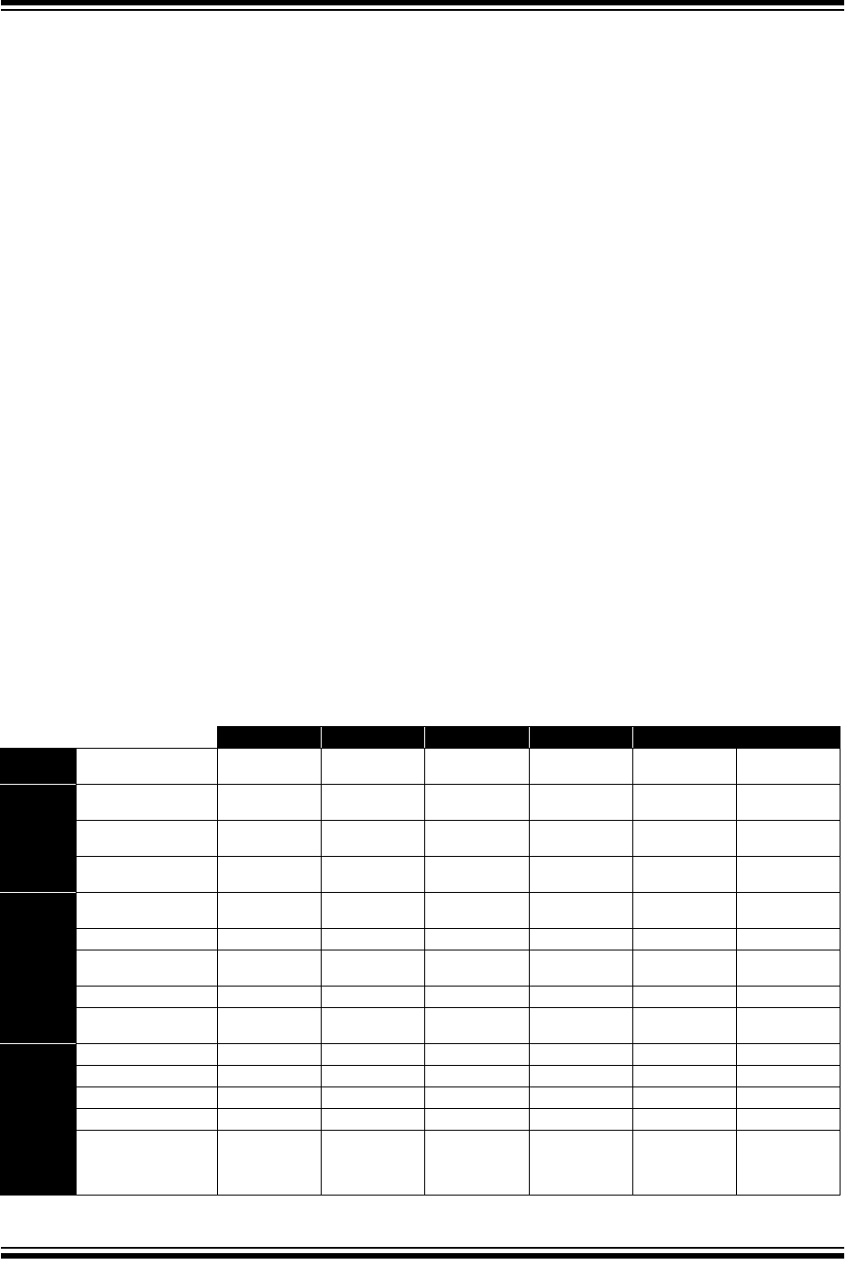
Table 1-1 shows the features of the PIC16F627A/
628A/648A mid-range microcontroller families.
A simplified block diagram of the PIC16F627A/628A/
648A is shown in Figure 3-1.
The PIC16F627A/628A/648A series fits in applications
ranging from battery chargers to low power remote
sensors. The FLASH technology makes customizing
application programs (detection levels, pulse genera-
tion, timers, etc.) extremely fast and convenient. The
small footprint packages makes this microcontroller
series ideal for all applications with space limitations.
Low cost, low power, high performance, ease of use
and I/O flexibility make the PIC16F627A/628A/648A
very versatile.
1.1 Development Support
The PIC16F627A/628A/648A family is supported by a
full-featured macro assembler, a software simulator, an
in-circuit emulator, a low cost in-circuit debugger, a low
cost development programmer and a full-featured pro-
grammer. A Third Party “C” compiler support tool is
also available.
TABLE 1-1: PIC16F627A/628A/648A FAMILY OF DEVICES
PIC16F627A PIC16F628A PIC16F648A PIC16LF627A PIC16LF628A PIC16LF648A
Clock Maximum Frequency
of Operation (MHz)
20 20 20 4 4 4
FLASH Program Mem-
ory (words)
1024 2048 4096 1024 2048 4096
Memory RAM Data Memory
(bytes)
224 224 256 224 224 256
EEPROM Data Mem-
ory (bytes)
128 128 256 128 128 256
Timer module(s) TMR0, TMR1,
TMR2
TMR0, TMR1,
TMR2
TMR0, TMR1,
TMR2
TMR0, TMR1,
TMR2
TMR0, TMR1,
TMR2
TMR0, TMR1,
TMR2
Comparator(s) 222222
Peripherals Capture/Compare/
PWM modules
111111
Serial Communications USART USART USART USART USART USART
Internal Voltage
Reference
Yes Yes Yes Yes Yes Yes
Interrupt Sources 10 10 10 10 10 10
I/O Pins 16 16 16 16 16 16
Features Voltage Range (Volts) 3.0-5.5 3.0-5.5 3.0-5.5 2.0-5.5 2.0-5.5 2.0-5.5
Brown-out Reset Yes Yes Yes Yes Yes Yes
Packages 18-pin DIP,
SOIC, 20-pin
SSOP,
28-pin QFN
18-pin DIP,
SOIC, 20-pin
SSOP,
28-pin QFN
18-pin DIP,
SOIC, 20-pin
SSOP,
28-pin QFN
18-pin DIP,
SOIC, 20-pin
SSOP,
28-pin QFN
18-pin DIP,
SOIC, 20-pin
SSOP,
28-pin QFN
18-pin DIP,
SOIC, 20-pin
SSOP,
28-pin QFN
All PICmicro® Family devices have Power-on Reset, selectable Watchdog Timer, selectable Code Protect and high I/O current capability.
All PIC16F627A/628A/648A Family devices use serial programming with clock pin RB6 and data pin RB7.