
Datasheet


Table Of Contents
- High Performance RISC CPU:
- Special Microcontroller Features:
- Low Power Features:
- Peripheral Features:
- Pin Diagrams
- Most Current Data Sheet
- Errata
- Customer Notification System
- 1.0 General Description
- 2.0 PIC16F627A/628A/648A Device Varieties
- 3.0 Architectural Overview
- 4.0 Memory Organization
- FIGURE 4-1: Program Memory Map and Stack
- TABLE 4-1: general purpose STATIC ram Registers
- TABLE 4-2: Access to Banks of Registers
- FIGURE 4-2: Data Memory Map of the PIC16F627A and PIC16F628A
- FIGURE 4-3: Data Memory Map of the PIC16F648A
- TABLE 4-3: Special Registers Summary Bank0
- TABLE 4-4: Special Function Registers Summary Bank1
- TABLE 4-5: Special Function Registers Summary Bank2
- TABLE 4-6: Special Function Registers Summary Bank3
- FIGURE 4-4: Loading Of PC In Different Situations
- FIGURE 4-5: Direct/Indirect Addressing PIC16F627A/628A/648A
- 5.0 I/O Ports
- FIGURE 5-1: Block Diagram of RA0/AN0:RA1/AN1 Pins
- FIGURE 5-2: Block Diagram of RA2/Vref Pin
- FIGURE 5-3: Block Diagram of the RA3/AN3 Pin
- FIGURE 5-4: Block Diagram of RA4/T0CKI Pin
- FIGURE 5-5: Block Diagram of the RA5/MCLR/Vpp Pin
- FIGURE 5-6: Block Diagram of RA6/OSC2/CLKOUT Pin
- FIGURE 5-7: Block Diagram of RA7/OSC1/CLKIN Pin
- TABLE 5-1: PORTA Functions
- TABLE 5-2: Summary of Registers Associated with PORTA(1)
- FIGURE 5-8: Block Diagram of RB0/INT Pin
- FIGURE 5-9: Block Diagram of RB1/RX/DT Pin
- FIGURE 5-10: Block Diagram of RB2/TX/CK Pin
- FIGURE 5-11: Block Diagram of RB3/CCP1 Pin
- FIGURE 5-12: Block Diagram of RB4/PGM Pin
- FIGURE 5-13: Block Diagram of RB5 Pin
- FIGURE 5-14: Block Diagram of RB6/T1OSO/T1CKI Pin
- FIGURE 5-15: Block Diagram of the RB7/T1OSI Pin
- TABLE 5-3: PORTB Functions
- TABLE 5-4: Summary of Registers Associated With PORTB(1)
- FIGURE 5-16: Successive I/O Operation
- 6.0 Timer0 Module
- 7.0 Timer1 Module
- 8.0 Timer2 Module
- 9.0 Capture/Compare/PWM (CCP) Module
- TABLE 9-1: CCP Mode - Timer Resource
- FIGURE 9-1: Capture Mode Operation Block Diagram
- FIGURE 9-2: Compare Mode Operation Block Diagram
- TABLE 9-2: Registers Associated with Capture, compare, and Timer1
- FIGURE 9-3: Simplified PWM Block Diagram
- FIGURE 9-4: PWM OUTPUT
- TABLE 9-3: Example PWM Frequencies and Resolutions at 20 MHz
- TABLE 9-4: Registers Associated with PWM and Timer2
- 10.0 Comparator Module
- 11.0 Voltage Reference Module
- 12.0 Universal Synchronous Asynchronous Receiver Transmitter (USART) Module
- TABLE 12-1: BAUD rATE fORMULA
- TABLE 12-2: Registers Associated with Baud Rate Generator
- TABLE 12-3: Baud Rates for synchronous Mode
- TABLE 12-4: Baud Rates for Asynchronous Mode (BRGH = 0)
- TABLE 12-5: Baud Rates for Asynchronous Mode (BRGH = 1)
- FIGURE 12-1: RX Pin Sampling Scheme. BRGH = 0
- FIGURE 12-2: RX Pin Sampling Scheme, BRGH = 1
- FIGURE 12-3: RX Pin Sampling Scheme, BRGH = 1
- FIGURE 12-4: RX Pin Sampling Scheme, BRGH = 0 OR BRGH = 1
- FIGURE 12-5: USART Transmit Block Diagram
- FIGURE 12-6: Asynchronous Transmission
- FIGURE 12-7: Asynchronous Transmission (Back to Back)
- TABLE 12-6: Registers Associated with Asynchronous Transmission
- FIGURE 12-8: USART Receive Block Diagram
- FIGURE 12-9: Asynchronous Reception with Address Detect
- FIGURE 12-10: Asynchronous Reception with Address Byte First
- FIGURE 12-11: Asynchronous Reception with Address Byte First Followed by Valid Data Byte
- TABLE 12-7: Registers Associated with Asynchronous Reception
- TABLE 12-8: Registers Associated with Asynchronous Reception
- TABLE 12-9: Registers Associated with Synchronous Master Transmission
- FIGURE 12-12: Synchronous Transmission
- FIGURE 12-13: Synchronous Transmission (Through TXEN)
- TABLE 12-10: Registers Associated with Synchronous Master Reception
- FIGURE 12-14: Synchronous Reception (Master Mode, SREN)
- TABLE 12-11: Registers Associated with Synchronous Slave Transmission
- TABLE 12-12: Registers Associated with Synchronous Slave Reception
- 13.0 Data EEPROM Memory
- 14.0 Special Features of the CPU
- FIGURE 14-1: Crystal Operation (or Ceramic Resonator) (HS, XT or LP Osc Configuration)
- TABLE 14-1: Capacitor Selection for Ceramic Resonators
- TABLE 14-2: Capacitor Selection for Crystal Oscillator
- FIGURE 14-2: External Parallel Resonant Crystal Oscillator Circuit
- FIGURE 14-3: External Series Resonant Crystal Oscillator Circuit
- FIGURE 14-4: External Clock Input Operation (EC, HS, XT or LP Osc Configuration)
- FIGURE 14-5: RC OSCILLATOR MODE
- FIGURE 14-6: Simplified Block Diagram of On-chip Reset Circuit
- FIGURE 14-7: Brown-out Situations WITH PWRT ENABLED
- TABLE 14-3: Time out in Various Situations
- TABLE 14-4: Status/PCON Bits and Their Significance
- TABLE 14-5: Summary of Registers Associated with Brown-out Reset
- TABLE 14-6: Initialization Condition for Special Registers
- TABLE 14-7: Initialization Condition for Registers
- FIGURE 14-8: Time out Sequence on Power-up (MCLR not tied to Vdd): Case
- FIGURE 14-9: Time out Sequence on Power-up (MCLR not tied to Vdd): Case 2
- FIGURE 14-10: Time out Sequence on Power-up (MCLR tied to Vdd)
- FIGURE 14-11: External Power-on Reset Circuit (For Slow Vdd Power-up)
- FIGURE 14-12: External Brown-out Protection Circuit 1
- FIGURE 14-13: External Brown-out Protection Circuit 2
- FIGURE 14-14: Interrupt Logic
- FIGURE 14-15: INT Pin Interrupt Timing
- TABLE 14-8: Summary of interrupt registers
- FIGURE 14-16: Watchdog Timer Block Diagram
- TABLE 14-9: Summary of Watchdog Timer Registers
- FIGURE 14-17: Wake-up from Sleep Through Interrupt
- FIGURE 14-18: Typical In-Circuit Serial Programming Connection
- 15.0 Instruction Set Summary
- 16.0 Development Support
- 17.0 Electrical Specifications
- FIGURE 17-1: PIC16F627A/628A/648A VOLTAGE-FREQUENCY GRAPH, -40°C £ TA £ +125°C
- FIGURE 17-2: PIC16LF627A/628A/648A VOLTAGE-FREQUENCY GRAPH, -40°C £ TA £ +85°C
- TABLE 17-1: DC Characteristics: PIC16F627A/628A/648A (Industrial, Extended) PIC16LF627A/628A/648A...
- TABLE 17-2: Comparator Specifications
- TABLE 17-3: Voltage Reference Specifications
- FIGURE 17-3: Load Conditions
- FIGURE 17-4: External Clock Timing
- TABLE 17-4: External Clock Timing Requirements
- TABLE 17-5: pRECISION INTERNAL OSCILLATOR Parameters
- FIGURE 17-5: CLKOUT and I/O Timing
- TABLE 17-6: CLKOUT and I/O Timing Requirements
- FIGURE 17-6: Reset, Watchdog Timer, Oscillator Start-Up Timer and Power-Up Timer Timing
- FIGURE 17-7: Brown-out Detect Timing
- TABLE 17-7: Reset, Watchdog Timer, Oscillator Start-up Timer and Power-up Timer Requirements
- FIGURE 17-8: Timer0 and Timer1 External Clock Timings
- TABLE 17-9: Timer0 and Timer1 External Clock Requirements
- FIGURE 17-10: Capture/Compare/PWM Timings
- TABLE 17-8: Capture/Compare/PWM Requirements
- FIGURE 17-11: TIMER0 Clock Timing
- TABLE 17-9: TIMER0 Clock Requirements
- 18.0 DC and AC Characteristics Graphs and Tables
- 19.0 Packaging Information
- Appendix A: Data Sheet Revision History
- Appendix B: Device Differences
- Appendix C: Device Migrations
- Appendix D: Migrating from other PICmicro Devices
- Appendix E: Development Tool Version Requirements
- Index
- Product ID System
- Worldwide Sales
2002 Microchip Technology Inc. Preliminary DS40044A-page 111
PIC16F627A/628A/648A
15.0 INSTRUCTION SET SUMMARY
Each PIC16F627A/628A/648A instruction is a 14-bit
word divided into an OPCODE which specifies the
instruction type and one or more operands which fur-
ther specify the operation of the instruction. The
PIC16F627A/628A/648A instruction set summary in
Table 15-2 lists byte-oriented, bit-oriented, and lit-
eral and control operations. Table 15-1 shows the
opcode field descriptions.
For byte-oriented instructions, 'f' represents a file
register designator and 'd' represents a destination
designator. The file register designator specifies which
file register is to be used by the instruction.
The destination designator specifies where the result of
the operation is to be placed. If 'd' is zero, the result is
placed in the W register. If 'd' is one, the result is placed
in the file register specified in the instruction.
For bit-oriented instructions, 'b' represents a bit field
designator which selects the number of the bit affected
by the operation, while 'f' represents the number of the
file in which the bit is located.
For literal and control operations, 'k' represents an
eight or eleven bit constant or literal value.
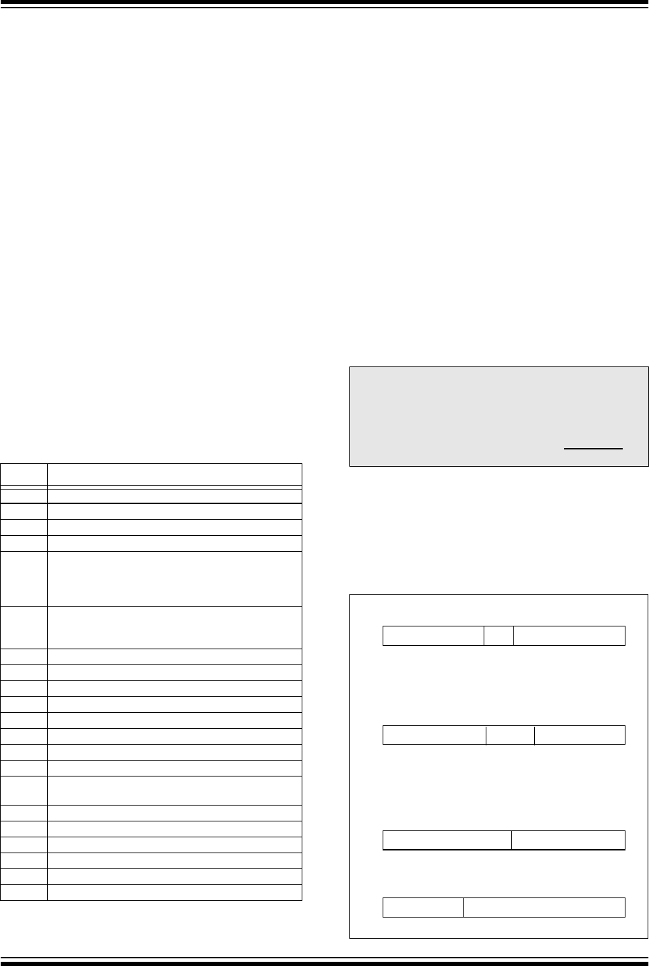
TABLE 15-1: OPCODE FIELD
DESCRIPTIONS
The instruction set is highly orthogonal and is grouped
into three basic categories:
• Byte-oriented operations
• Bit-oriented operations
• Literal and control operations
All instructions are executed within one single
instruction cycle, unless a conditional test is true or the
program counter is changed as a result of an
instruction. In this case, the execution takes two
instruction cycles with the second cycle executed as a
NOP. One instruction cycle consists of four oscillator
periods. Thus, for an oscillator frequency of 4 MHz, the
normal instruction execution time is 1 µs. If a
conditional test is true or the program counter is
changed as a result of an instruction, the instruction
execution time is 2 µs.
Table 15-2 lists the instructions recognized by the
MPASM™ assembler.
Figure 15-1 shows the three general formats that the
instructions can have.
All examples use the following format to represent a
hexadecimal number:
0xhh
where h signifies a hexadecimal digit.
FIGURE 15-1: GENERAL FORMAT FOR
INSTRUCTIONS
Field Description
f Register file address (0x00 to 0x7F)
W Working register (accumulator)
b Bit address within an 8-bit file register
k Literal field, constant data or label
x Don't care location (= 0 or 1)
The assembler will generate code with x = 0. It is the
recommended form of use for compatibility with all
Microchip software tools.
d Destination select; d = 0: store result in W,
d = 1: store result in file register f.
Default is d = 1
label Label name
TOS Top of Stack
PC Program Counter
PCLATH Program Counter High Latch
GIE Global Interrupt Enable bit
WDT Watchdog Timer/Counter
TO Time out bit
PD Power-down bit
dest Destination either the W register or the specified regis-
ter file location
[ ] Options
( ) Contents
→ Assigned to
< > Register bit field
∈ In the set of
italics User defined term (font is courier)
Note 1: Any unused opcode is reserved. Use of
any reserved opcode may cause unex-
pected operation.
2: To maintain upward compatibility with
future PICmicro
products, do not use the
OPTION and TRIS instructions.
Byte-oriented file register operations
d = 0 for destination W
OPCODE d f (FILE #)
d = 1 for destination f
f = 7-bit file register address
Bit-oriented file register operations
OPCODE b (BIT #) f (FILE #)
b = 3-bit bit address
f = 7-bit file register address
Literal and control operations
OPCODE k (literal)
k = 8-bit immediate value
OPCODE k (literal)
k = 11-bit immediate value
General
CALL and GOTO instructions only
13 8 7 6 0
13 10 9 7 06
13 8 7 0
13 11 10 0