
Information

2000-2012 Microchip Technology Inc. DS80073H-page 5
PIC16F62X
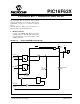
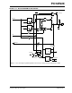
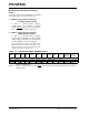
FIGURE 5-12: BLOCK DIAGRAM OF RB4/PGM PIN
Data Latch
TRIS Latch
RD TRISB
P
V
SS
Q
D
Q
CK
Q
D
Q
CK
N
VDD
RD PORTB
WR PORTB
WR TRISB
Schmitt
Trigger
PGM Input
LVP
Data Bus
RB4/PGM
RBPU
VDD
Weak Pull-up
P
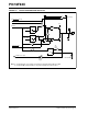
From other
QD
EN
QD
EN
Set RBIF
RB<7:4> pins
RD Port
Q3
Q1
TTL
Input
Buffer
VDD
VSS
Note 1: The Low-Voltage Programming disables the interrupt-on-change and the weak pull-ups on RB4.