
Information


PIC16F62X
DS80073H-page 14 2000-2012 Microchip Technology Inc.
6. Module: Timer1 Module
In Section 7.0, “Timer1 Module”, in Register 7-1,
bit TMR1ON, “Timer1 On” should read as shown in
bold below:
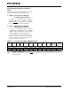
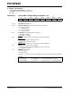
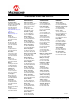
REGISTER 7-1: T1CON: TIMER1 CONTROL REGISTER (ADDRESS: 10h)
U-0 U-0 R/W-0 R/W-0 R/W-0 R/W-0 R/W-0 R/W-0
— — T1CKPS1 T1CKPS0 T1OSCEN T1SYNC TMR1CS TMR1ON
bit 7 bit 0
bit 7-6 Unimplemented: Read as ‘0’
bit 5-4 T1CKPS1/T1CKPS0: Timer1 Input Clock Prescale Select bits
11 = 1:8 prescale value
10 = 1:4 prescale value
01 = 1:2 prescale value
11 = 1:1 prescale value
bit 3 T1OSCEN: Timer1 Oscillator Enable Control bit
1 = Oscillator is enabled
0 = Oscillator is shut off
(1)
bit 2 T1SYNC: Timer1 External Clock Input Synchronization Control bit
TMR1CS =
1
1 = Do not synchronize external clock input
0 = Synchronize external clock input
TMR1CS =
0
This bit is ignored. Timer1 uses the internal clock when TRM1CS = 0.
bit 1 TMR1CS: Timer1 Clock Source Select bit
1 = External clock from pin RB6/T1OSO/T1CKI (on the rising edge)
0 = Internal clock (FOSC/4)
bit 0 TMR1ON: Timer1 On bit
1 = Enables Timer1
0 = Disables Timer1
Note 1: The oscillator inverter and feedback resistor are turned off to eliminate power drain.
Legend:
R = Readable bit W = Writable bit U = Unimplemented bit, read as ‘0’
-n = Value at POR ‘1’ = Bit is set ‘0’ = Bit is cleared x = Bit is unknown