
Information

2000-2012 Microchip Technology Inc. DS80073H-page 13
PIC16F62X
5. Module: Data EEPROM Memory
Examples 13-1, “Data EEPROM Read”, 13-2,
“Data EEPROM Write”, and 13-3, “Write Verify”,
are incorrect. The EEPROM registers are all
located in Bank 1. The examples show the regis-
ters in Bank 0 and Bank 1. The following code
examples should be used instead.
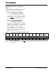
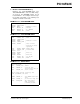
EXAMPLE 13-1: DATA EEPROM READ
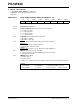
EXAMPLE 13-2: DATA EEPROM WRITE
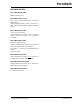
EXAMPLE 13-3: WRITE VERIFY
BSF STATUS, RP0 ; Bank 1
MOVLW CONFIG_ADDR ;
MOVWF EEADR ; Address to write
BSF EECON1, RD ; EE Read
MOVF EEDATA, W ; W = EEDATA
BCF STATUS, RP0 ; Bank 0
; set up the data and the address
BSF STATUS, RP0 ; Bank 1
MOVLW CONFIG_ADDR ;
MOVWF EEADR ; Address to write
MOVLW CONFIG_DATA ;
MOVWF EEDATA ; Data to write
; perform the write
operation
BSF EECON1, WREN ; Enable Write
BCF INTCON, GIE ; Disable INTs
MOVLW 055h ;
MOVWF EECON2 ; Write 55
MOVLW 0AAh ;
MOVWF EECON2 ; Write AA
BSF EECON1, WR ; Set WR bit
BCF STATUS, RP0 ; Bank 0
; after the write in complete (i.e. in the
write interrupt)
BSF STATUS, RP0 ; Bank 1
MOVF EEDATA, W ; load the last
written value into W
BSF EECON1, RD ; start a read
;
; Is the value written (in W Reg) and
; read (in EEDATA) the same?
;
SUBWF EEDATA, W ; the EEDATA has fresh
data
BTFSS STATUS, Z ; Is the Zero flag set?
GOTO WRITE_ERR ; NO, Write Error
; YES, Good Write
; continue program