
Information

PIC16F62X
DS80073H-page 10 2000-2012 Microchip Technology Inc.
Clarifications/Corrections to the Data
Sheet:
In the Device Data Sheet (DS40300C), the following
clarifications and corrections should be noted.
1. Module: Special Function Registers
(T1SYNC, Register T1CON)
In Table 3-1, “Special Function Registers
Summary Bank 0”, bit T1SYNC, in Register
T1CON (address 10h), should be asserted logic
low (i.e., T1SYNC
) as shown in bold below.
2. Module: Special Function Registers
(ADEN, Register RCSTA)
In Table 3-1, “Special Function Registers
Summary Bank 0”, bit ADEN, in Register RCSTA
(address 18h), is misspelled. The correct spelling
should be ADDEN, as shown in bold below.
This misspelling also appears in Register 12-2.
Tables 12-2, 12-6, 12-7, 12-8, 12-9, 12-10, 12-11
and 12-12. Figures 12-8, 12-9, 12-10 and 12-11.
Sections 12.2.2, 12.3.1 and 12.3.1.1.
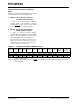
TABLE 3-1: SPECIAL REGISTERS SUMMARY BANK 0
Address Name Bit 7 Bit 6 Bit 5 Bit 4 Bit 3 Bit 2 Bit 1 Bit 0
Value on
POR Reset
Value on all
other
Resets
(1)
Bank 0
10h T1CON
— — T1CKPS1 T1CKPS0 T1OSCEN T1SYNC TMR1CS TMR1ON --00 0000 --uu uuuu
18h RCSTA SPEN RX9 SREN CREN ADDEN FERR OERR RX9D 0000 -00x 0000 -00x
Legend: x = unknown, u = unchanged, - = unimplemented locations, read as ‘0’, q = value depends on condition,
shaded = unimplemented
Note 1: Other (non power-up) Resets include MCLR
Reset, Brown-out Reset and Watchdog Timer Reset during
normal operation.