PIC16F62X PIC16F62X Rev. C Silicon/Data Sheet Errata The PIC16F62X (Rev. C) parts you have received conform functionally to the Device Data Sheet (DS40300C), except for the anomalies described below. Microchip intends to address all issues listed here in future revisions of the PIC16F62X silicon. 1. Module: I/O Ports A read of the PORTB Data Direction Register (TRISB) returns the Data Direction state on the port pins themselves and not the contents of the TRISB register latch.
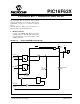
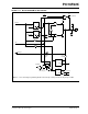
PIC16F62X FIGURE 5-9: BLOCK DIAGRAM OF RB1/RX/DT PIN VDD RBPU P Weak Pull-up Port/Peripheral Select(1) USART Data Output 0 VDD 1 Data Bus WR PORTB D Q CK Q P VDD Data Latch WR TRISB D Q CK Q RB1/RX/DT pin N VSS TRIS Latch VSS RD TRISB TTL Input Buffer Peripheral OE(2) Q D RD PORTB EN USART Receive Input RD PORTB Schmitt Trigger Note 1: Port/Peripheral select signal selects between port data and peripheral output.
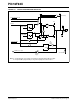
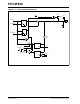
PIC16F62X FIGURE 5-10: BLOCK DIAGRAM OF RB2/TX/CK PIN VDD RBPU P Weak Pull-up VDD Port/Peripheral Select(1) USART TX/CK Output 0 VDD 1 Data Bus WR PORTB D Q CK Q RB2/TX/CK pin P VSS Data Latch WR TRISB D Q CK Q N TRIS Latch Vss RD TRISB TTL Input Buffer Peripheral OE(2) Q D RD PORTB EN EN USART Slave Clock In Schmitt Trigger RD PORTB Note 1: Port/Peripheral select signal selects between port data and peripheral output.
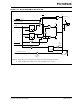
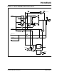
PIC16F62X FIGURE 5-11: BLOCK DIAGRAM OF RB3/CCP1 PIN VDD RBPU P Weak Pull-up Port/Peripheral Select(1) PWM/Compare Output 0 VDD 1 Data Bus WR PORTB D Q CK Q P VDD Data Latch D WR TRISB CK RB3/CCP1 pin Q N Q VSS TRIS Latch Vss RD TRISB TTL Input Buffer Q D RD PORTB EN EN CCP Input Schmitt Trigger RD PORTB Note 1: Peripheral select is defined by CCP1M3:CCP1M0 (CCP1CON<3:0>). DS80073H-page 4 2000-2012 Microchip Technology Inc.
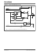
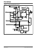
PIC16F62X FIGURE 5-12: BLOCK DIAGRAM OF RB4/PGM PIN VDD RBPU P Weak Pull-up VDD Data Bus WR PORTB D Q CK Q P VDD Data Latch WR TRISB D Q CK Q RB4/PGM N VSS TRIS Latch VSS RD TRISB LVP RD PORTB PGM Input TTL Input Buffer Schmitt Trigger Q D EN Q1 Set RBIF From other RB<7:4> pins Q D RD Port EN Q3 Note 1: The Low-Voltage Programming disables the interrupt-on-change and the weak pull-ups on RB4. 2000-2012 Microchip Technology Inc.
PIC16F62X FIGURE 5-13: BLOCK DIAGRAM OF RB5 PIN VDD RBPU Data Bus D Weak P Pull-up VDD Q RB5 pin WR PORTB CK Data Latch VSS D WR TRISB Q CK TRIS Latch TTL Input Buffer RD TRISB Q D RD PORTB EN Q1 Set RBIF From other RB<7:4> pins Q D RD Port EN DS80073H-page 6 Q3 2000-2012 Microchip Technology Inc.
PIC16F62X FIGURE 5-14: BLOCK DIAGRAM OF RB6/T1OSO/T1CKI PIN VDD RBPU P Weak Pull-up VDD Data Bus WR PORTB D Q CK Q P VDD Data Latch WR TRISB D Q CK Q RB6/ T1OSO/ T1CKI pin N VSS TRIS Latch VSS RD TRISB T1OSCEN TTL Input Buffer RD PORTB TMR1 Clock From RB7 Schmitt Trigger TMR1 Oscillator Serial Programming Clock Q D EN Q1 Set RBIF From other RB<7:4> pins Q D RD Port EN 2000-2012 Microchip Technology Inc.
PIC16F62X FIGURE 5-15: BLOCK DIAGRAM OF RB7/T1OSI PIN VDD RBPU TMR1 Oscillator P Weak Pull-up To RB6 T1OSCEN VDD VDD Data Bus WR PORTB D Q CK Q P RB7/T1OSI pin Data Latch WR TRISB D Q CK Q VSS N TRIS Latch Vss RD TRISB T10SCEN TTL Input Buffer RD PORTB Serial Programming Input Schmitt Trigger Q D EN Q1 Set RBIF From other RB<7:4> pins Q D RD Port EN DS80073H-page 8 Q3 2000-2012 Microchip Technology Inc.
PIC16F62X 2. Module: Comparator Mode 1 Mode 1 allows AN2 to drive the (+) inputs of both comparators. AN1 continues to drive the (-) input of Comparator 2, but AN0 and AN3 can be switched into the (-) input of Comparator 1. The state of the CIS bit chooses which input is to be connected to the comparator. When CIS = 0, AN0 is attached and the comparator functions correctly. When CIS = 1, AN3 is not completely connected to the comparator, resulting in incorrect behavior.
PIC16F62X Clarifications/Corrections to the Data Sheet: In the Device Data Sheet (DS40300C), the following clarifications and corrections should be noted. 1. Module: Special Function Registers (T1SYNC, Register T1CON) In Table 3-1, “Special Function Registers Summary Bank 0”, bit T1SYNC, in Register T1CON (address 10h), should be asserted logic low (i.e., T1SYNC) as shown in bold below. 2.
PIC16F62X 3. Module: I/O Ports (RA5/MCLR/VPP) Figure 5-5, “Block Diagram of the RA5/MCLR/VPP Pin”, is incorrect. The following diagram should be used instead. FIGURE 5-5: BLOCK DIAGRAM OF RA5/MCLR/VPP PIN MCLRE MCLR Circuit MCLR Filter(1) Program Mode VDD HV Detect RA5/MCLR/VPP VSS Data Bus Q D EN RD Port 2000-2012 Microchip Technology Inc.
PIC16F62X 4. Module: Comparator Example 9-1, “Initializing Comparator Module”, is incorrect. The following code example should be used instead.
PIC16F62X 5. Module: Data EEPROM Memory Examples 13-1, “Data EEPROM Read”, 13-2, “Data EEPROM Write”, and 13-3, “Write Verify”, are incorrect. The EEPROM registers are all located in Bank 1. The examples show the registers in Bank 0 and Bank 1. The following code examples should be used instead.
PIC16F62X 6. Module: Timer1 Module In Section 7.
PIC16F62X REVISION HISTORY Rev A Document (6/00) Original errata document. Rev B Document (11/00) Issue 3 (CCP Compare Mode), Table 1 and 2 were added (page 2). Under the Clarifications/Corrections Section, Item 1, Table 15-12 was updated with additional information (page 3). Rev C Document (6/01) Issues 2 and 3 were added. Under Clarifications/Corrections, Items 2 and 3 were changed and Item numbers were renumbered accordingly. Rev D Document (9/01) Item 3 was rewritten (page 9).
PIC16F62X NOTES: DS80073H-page 16 2000-2012 Microchip Technology Inc.
Note the following details of the code protection feature on Microchip devices: • Microchip products meet the specification contained in their particular Microchip Data Sheet. • Microchip believes that its family of products is one of the most secure families of its kind on the market today, when used in the intended manner and under normal conditions. • There are dishonest and possibly illegal methods used to breach the code protection feature.
Worldwide Sales and Service AMERICAS ASIA/PACIFIC ASIA/PACIFIC EUROPE Corporate Office 2355 West Chandler Blvd. Chandler, AZ 85224-6199 Tel: 480-792-7200 Fax: 480-792-7277 Technical Support: http://www.microchip.com/ support Web Address: www.microchip.