
Datasheet


PIC16(L)F1938/9
DS40001574C-page 382 2011-2013 Microchip Technology Inc.
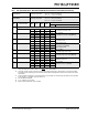
30.2 DC Characteristics: PIC16F/LF1938/39-I/E (Industrial, Extended)
PIC16LF1938/9
Standard Operating Conditions (unless otherwise stated)
Operating temperature -40°C TA +85°C for industrial
-40°C
TA +125°C for extended
PIC16F1938/9
Standard Operating Conditions (unless otherwise stated)
Operating temperature -40°C TA +85°C for industrial
-40°C
TA +125°C for extended
Param
No.
Device
Characteristics
Min. Typ† Max. Units
Conditions
V
DD Note
Supply Current (I
DD)
(1, 2)
D009
LDO Regulator
— 350 — A — HS, EC OR INTOSC/INTOSCIO (8-16 MHZ)
Clock modes with all V
CAP pins disabled
— 50
—
A — All VCAP pins disabled
— 30
—
A — VCAP enabled on RA0, RA5 or RA6
— 5
—
A — LP Clock mode and Sleep (requires FVR and
BOR to be disabled)
D010 — 5.2 16
A1.8FOSC = 32 kHz
LP Oscillator mode
(Note 4),
-40°C
TA +85°C
—7.6
20
A3.0
D010 — 26 45 A 1.8 FOSC = 32 kHz
LP Oscillator mode
(Note 4, 5),
-40°C
TA +85°C
— 32
50
A 3.0
— 35
55
A 5.0
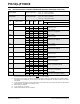
D010A — 5.2
16
A1.8
F
OSC = 32 kHz
LP Oscillator mode
(Note 4)
-40°C TA +125°C
—7.6
20
A3.0
D010A — 26
55
A 1.8
FOSC = 32 kHz
LP Oscillator mode
(Note 4, 5)
-40°C TA +125°C
— 32
70
A 3.0
— 35
75
A 5.0
D011 — 54
130
A1.8FOSC = 1 MHz
XT Oscillator mode
—110
170
A3.0
D011 — 80
150
A 1.8 FOSC = 1 MHz
XT Oscillator mode
(Note 5)
— 140
210
A 3.0
— 190
280
A 5.0
D012 — 200
300
A1.8FOSC = 4 MHz
XT Oscillator mode
— 350
480
A3.0
D012 — 220
320
A 1.8 FOSC = 4 MHz
XT Oscillator mode
(Note 5)
— 390
520
A 3.0
— 470
630
A 5.0
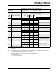
Note 1: The test conditions for all IDD measurements in active operation mode are: OSC1 = external square wave, from
rail-to-rail; all I/O pins tri-stated, pulled to V
DD; MCLR = VDD; WDT disabled.
2: The supply current is mainly a function of the operating voltage and frequency. Other factors, such as I/O pin loading
and switching rate, oscillator type, internal code execution pattern and temperature, also have an impact on the current
consumption.
3: For RC oscillator configurations, current through REXT is not included. The current through the resistor can be extended
by the formula I
R = VDD/2REXT (mA) with REXT in k
4:
FVR and BOR are disabled.
5: 0.1 F capacitor on VCAP (RA0).
6: 8 MHz crystal oscillator with 4x PLL enabled.