
Datasheet


PIC16(L)F1938/9
DS40001574C-page 156 2011-2013 Microchip Technology Inc.
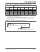
REGISTER 15-2: ADCON1: A/D CONTROL REGISTER 1
R/W-0/0 R/W-0/0 R/W-0/0 R/W-0/0 U-0 R/W-0/0 R/W-0/0 R/W-0/0
ADFM ADCS<2:0>
— ADNREF ADPREF<1:0>
bit 7 bit 0
Legend:
R = Readable bit W = Writable bit U = Unimplemented bit, read as ‘0’
u = Bit is unchanged x = Bit is unknown -n/n = Value at POR and BOR/Value at all other Resets
‘1’ = Bit is set ‘0’ = Bit is cleared
bit 7
ADFM: A/D Result Format Select bit
1 = Right justified. Six Most Significant bits of ADRESH are set to ‘0’ when the conversion result is
loaded.
0 = Left justified. Six Least Significant bits of ADRESL are set to ‘0’ when the conversion result is
loaded.
bit 6-4
ADCS<2:0>: A/D Conversion Clock Select bits
111 =F
RC (clock supplied from a dedicated RC oscillator)
110 =F
OSC/64
101 =F
OSC/16
100 =F
OSC/4
011 =F
RC (clock supplied from a dedicated RC oscillator)
010 =F
OSC/32
001 =F
OSC/8
000 =F
OSC/2
bit 3
Unimplemented: Read as ‘0’
bit 2
ADNREF: A/D Negative Voltage Reference Configuration bit
1 =V
REF- is connected to external VREF- pin
(1)
0 =VREF- is connected to VSS
bit 1-0 ADPREF<1:0>: A/D Positive Voltage Reference Configuration bits
11 =V
REF+ is connected to internal Fixed Voltage Reference (FVR) module
(1)
10 =VREF+ is connected to external VREF+ pin
(1)
01 = Reserved
00 =V
REF+ is connected to VDD
Note 1: When selecting the FVR or the VREF+ pin as the source of the positive reference, be aware that a
minimum voltage specification exists. See the applicable Electrical Specifications Chapter for details.