
Datasheet


2011-2013 Microchip Technology Inc. DS40001574C-page 231
PIC16(L)F1938/9
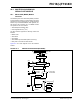
REGISTER 23-4: CCPxAS: CCPX AUTO-SHUTDOWN CONTROL REGISTER
R/W-0/0 R/W-0/0 R/W-0/0 R/W-0/0 R/W-0/0 R/W-0/0 R/W-0/0 R/W-0/0
CCPxASE CCPxAS2 CCPxAS1 CCPxAS0 PSSxAC<1:0> PSSxBD<1:0>
bit 7 bit 0
Legend:
R = Readable bit W = Writable bit U = Unimplemented bit, read as ‘0’
u = Bit is unchanged x = Bit is unknown -n/n = Value at POR and BOR/Value at all other Resets
‘1’ = Bit is set ‘0’ = Bit is cleared
bit 7
CCPxASE: CCPx Auto-Shutdown Event Status bit
1 = A shutdown event has occurred; CCPx outputs are in shutdown state
0 = CCPx outputs are operating
bit 6
CCPxAS2: CCPx Auto-Shutdown Source 2 Select bit
1 = Auto-shutdown 2 source is enabled, V
IL on INT pin
0 = Auto-shutdown 2 source is disabled
bit 5
CCPxAS1: CCPx Auto-Shutdown Source 1 Select bit
1 = Auto-shutdown 1 source is enabled, async_CxOUT
(1),(2)
output low
0 = Auto-shutdown 1 source is disabled
bit 4
CCPxAS0: CCPx Auto-Shutdown Source 0 Select bit
1 = Auto-shutdown 0 source is enabled, async_C1OUT
(1)
output low
0 = Auto-shutdown 0 source is disabled
bit 3-2
PSSxAC<1:0>: Pins PxA and PxC Shutdown State Control bits
00 = Drive pins PxA and PxC to ‘0’
01 = Drive pins PxA and PxC to ‘1’
1x = Pins PxA and PxC tri-state
bit 1-0
PSSxBD<1:0>: Pins PxB and PxD Shutdown State Control bits
00 = Drive pins PxB and PxD to ‘0’
01 = Drive pins PxB and PxD to ‘1’
1x = Pins PxB and PxD tri-state
Note 1: If CxSYNC is enabled, the shutdown will be delayed by Timer1.
2: async_CxOUT = async_C2OUT (for CCP1 and CCP2)
async_CxOUT = async_C3OUT (for CCP3)