
Datasheet


2011-2013 Microchip Technology Inc. DS40001574C-page 207
PIC16(L)F1938/9
23.1.6 ALTERNATE PIN LOCATIONS
This module incorporates I/O pins that can be moved to
other locations with the use of the alternate pin function
register, APFCON. To determine which pins can be
moved and what their default locations are upon a
Reset, see
Section 12.1 “Alternate Pin Function” for
more information.
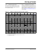
TABLE 23-2: SUMMARY OF REGISTERS ASSOCIATED WITH CAPTURE
Name Bit 7 Bit 6 Bit 5 Bit 4 Bit 3 Bit 2 Bit 1 Bit 0
Register
on Page
APFCON — CCP3SEL T1GSEL P2BSEL SRNQSEL
C2OUTSEL
SSSEL CCP2SEL 123
CCPxCON
PxM<1:0>
(1)
DCxB<1:0> CCPxM<3:0>
228
CCPRxL Capture/Compare/PWM Register x Low Byte (LSB)
206
CCPRxH Capture/Compare/PWM Register x High Byte (MSB)
206
INTCON GIE PEIE
TMR0IE INTE IOCIE TMR0IF INTF IOCIF
90
PIE1 TMR1GIE ADIE RCIE TXIE SSPIE CCP1IE TMR2IE TMR1IE
91
PIE2 OSFIE C2IE C1IE EEIE BCLIE LCDIE — CCP2IE
92
PIE3
— CCP5IE CCP4IE CCP3IE TMR6IE — TMR4IE —
93
PIR1 TMR1GIF ADIF RCIF TXIF SSPIF CCP1IF TMR2IF TMR1IF
94
PIR2
OSFIF C2IF C1IF EEIF BCLIF LCDIF —CCP2IF
95
PIR3 — CCP5IF CCP4IF CCP3IF TMR6IF — TMR4IF —
95
T1CON TMR1CS<1:0> T1CKPS<1:0> T1OSCEN T1SYNC —TMR1ON
197
T1GCON TMR1GE T1GPOL T1GTM T1GSPM T1GGO/DONE T1GVAL T1GSS<1:0>
198
TMR1L Holding Register for the Least Significant Byte of the 16-bit TMR1 Register
193
TMR1H Holding Register for the Most Significant Byte of the 16-bit TMR1 Register
193
TRISA
TRISA7 TRISA6 TRISA5 TRISA4 TRISA3 TRISA2 TRISA1 TRISA0
125
TRISB TRISB7 TRISB6 TRISB5 TRISB4 TRISB3 TRISB2 TRISB1 TRISB0
130
TRISC TRISC7 TRISC6 TRISC5 TRISC4 TRISC3 TRISC2 TRISC1 TRISC0
134
TRISD
(2)
TRISD7 TRISD6 TRISD5 TRISD4 TRISD3 TRISD2 TRISD1 TRISD0
137
TRISE
— — — — —
(3)
TRISE2
(2)
TRISE1
(2)
TRISE0
(2)
140
Legend: — = Unimplemented location, read as ‘0’. Shaded cells are not used by Capture mode.
Note 1: Applies to ECCP modules only.
2: These registers/bits are not implemented on PIC16(L)F1938 devices, read as ‘0’.
3: Unimplemented, read as ‘1’.