
Datasheet


PIC16(L)F1938/9
DS40001574C-page 170 2011-2013 Microchip Technology Inc.
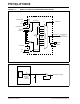
FIGURE 18-2: COMPARATOR MODULE SIMPLIFIED BLOCK DIAGRAM
Note 1: When CxON = 0, the Comparator will produce a ‘0’ at the output.
2: When CxON = 0, all multiplexer inputs are disconnected.
3: Output of comparator can be frozen during debugging.
MUX
Cx
(3)
0
1
2
3
CxON
(1)
CxNCH<1:0>
2
0
1
CXPCH<1:0>
C12IN1-
C12IN2-
C12IN3-
CXIN+
MUX
-
+
CxVN
CxVP
async_CxOUT
Q1
D
EN
Q
C
XPOL
Set CxIF
0
1
CXSYNC
CXOE
CXOUT
DQ
DAC Output
FVR Buffer2
C12IN0-
2
CxSP
CxHYS
det
Interrupt
det
Interrupt
to T1G MUX
CxINTN
CxINTP
2
3
VSS
TRIS bit
CxON
(2)
(2)
(from Timer1)
T1CLK
to CMxCON0 (CxOUT)
and CM2CON1 (MCxOUT)
to PWM
sync_CxOUT
and SR Latch