
Datasheet


2011-2013 Microchip Technology Inc. DS40001574C-page 149
PIC16(L)F1938/9
15.0 ANALOG-TO-DIGITAL
CONVERTER (ADC) MODULE
The Analog-to-Digital Converter (ADC) allows
conversion of an analog input signal to a 10-bit binary
representation of that signal. This device uses analog
inputs, which are multiplexed into a single sample and
hold circuit. The output of the sample and hold is
connected to the input of the converter. The converter
generates a 10-bit binary result via successive
approximation and stores the conversion result into the
ADC result registers (ADRESH:ADRESL register pair).
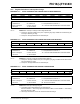
Figure 15-1 shows the block diagram of the ADC.
The ADC voltage reference is software selectable to be
either internally generated or externally supplied.
The ADC can generate an interrupt upon completion of
a conversion. This interrupt can be used to wake-up the
device from Sleep.
FIGURE 15-1: ADC BLOCK DIAGRAM
DAC_output
VDD
VREF+
ADPREF =
10
ADPREF = 00
ADPREF = 11
FVR Buffer1
VSS
VREF-
ADNREF =
1
ADNREF = 0
Note 1: When ADON = 0, all multiplexer inputs are disconnected.
2: Not available on PIC16(L)F1938.
ADON
(1)
GO/DONE
VSS
ADC
00000
00001
00010
00011
00100
00101
00111
00110
01000
01001
01010
01011
01100
01101
11110
CHS<4:0>
AN0
AN1
V
REF-/AN2
AN4
AN5
(2)
AN6
(2)
AN7
(2)
VREF+/AN3
AN8
AN9
AN10
AN11
AN12
AN13
11111
ADRESH ADRESL
10
16
ADFM
0 = Left Justify
1 = Right Justify
Temperature Indicator
11101
Ref+
Ref-