
Datasheet


PIC16(L)F1938/9
DS40001574C-page 142 2011-2013 Microchip Technology Inc.
TABLE 12-13: SUMMARY OF REGISTERS ASSOCIATED WITH PORTE
REGISTER 12-22: WPUE: WEAK PULL-UP PORTE REGISTER
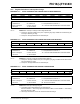
U-0 U-0 U-0 U-0 R/W-1/1 U-0 U-0 U-0
— — — —
WPUE3
— — —
bit 7 bit 0
Legend:
R = Readable bit W = Writable bit U = Unimplemented bit, read as ‘0’
u = Bit is unchanged x = Bit is unknown -n/n = Value at POR and BOR/Value at all other Resets
‘1’ = Bit is set ‘0’ = Bit is cleared
bit 7-4 Unimplemented: Read as ‘0’
bit 3 WPUE: Weak Pull-up Register bit
1 = Pull-up enabled
0 = Pull-up disabled
bit 2-0 Unimplemented: Read as ‘0’
Note 1: Global WPUEN
bit of the OPTION_REG register must be cleared for individual pull-ups to be enabled.
2: The weak pull-up device is automatically disabled if the pin is in configured as an output.
Name Bit 7 Bit 6 Bit 5 Bit 4 Bit 3 Bit 2 Bit 1 Bit 0
Register
on Page
ADCON0
—
CHS<4:0>
GO/DONE ADON
155
ANSELE
— — — — — ANSE2
(1)
ANSE1
(1)
ANSE0
(1)
141
CCPxCON
PxM<1:0> DCxB<1:0> CCPxM<3:0> 228
LATE
— — — — —LATE2
(1)
LATE1
(1)
LATE0
(1)
141
LCDCON LCDEN SLPEN WERR —
CS<1:0>
LMUX<1:0>
327
LCDSE2 SE23 SE22 SE21 SE20 SE19 SE18 SE17 SE16 331
PORTE
— — — —RE3RE2
(1)
RE1
(1)
RE0
(1)
140
TRISE
— — — —
—
(2)
TRISE2
(1)
TRISE1
(1)
TRISE0
(1)
140
WPUE
— — — — WPUE3 — — — 142
Legend: x = unknown, u = unchanged, – = unimplemented locations read as ‘0’. Shaded cells are not used by
PORTE.
Note 1: These bits are not implemented on the PIC16(L)F1938 devices, read as ‘0’.
2: Unimplemented, read as ‘1’.