
Datasheet


2011-2013 Microchip Technology Inc. DS40001574C-page 123
PIC16(L)F1938/9
12.2 Register Definitions: Alternate Pin Function Control
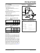
REGISTER 12-1: APFCON: ALTERNATE PIN FUNCTION CONTROL REGISTER
U-0 R/W-0/0 R/W-0/0 R/W-0/0 R/W-0/0 R/W-0/0 R/W-0/0 R/W-0/0
— CCP3SEL T1GSEL P2BSEL SRNQSEL
C2OUTSEL
SSSEL CCP2SEL
bit 7 bit 0
Legend:
R = Readable bit W = Writable bit U = Unimplemented bit, read as ‘0’
u = bit is unchanged x = Bit is unknown -n/n = Value at POR and BOR/Value at all other Resets
‘1’ = Bit is set ‘0’ = Bit is cleared
bit 7 Unimplemented: Read as ‘0’.
bit 6 CCP3SEL: CCP3 Input/Output Pin Selection bit
For 28-Pin Devices
(PIC16F1933/1936/1938):
0 = CCP3/P3A function is on RC6/TX/CK/CCP3/P3A/SEG9
1 = CCP3/P3A function is on RB5/AN13/CPS5/CCP3/P3A/T1G/COM1
For 40-Pin Devices
(PIC16F1934/1937/1939):
0 = CCP3/P3A function is on RE0/AN5/CCP3/P3A/SEG21
1 = CCP3/P3A function is on RB5/AN13/CPS5/CCP3/P3A/T1G/COM1
bit 5 T1GSEL: Timer1 Gate Input Pin Selection bit
0 = T1G function is on RB5/AN13/CPS5/CCP3/P3A/T1G/COM1
1 = T1G function is on RC4/SDI/SDA/T1G/SEG11
bit 4 P2BSEL: CCP2 PWM B Output Pin Selection bit
For 28-Pin Devices
(PIC16F1933/1936/1938):
0 = P2B function is on RC0/T1OSO/T1CKI/P2B
1 = P2B function is on RB5/AN13/P2B/CPS5/T1G/COM1
For 40-Pin Devices
(PIC16F1934/1937/1939):
0 = P2B function is on RC0/T1OSO/T1CKI/P2B
1 = P2B function is on RD2/CPS10/P2B
bit 3 SRNQSEL: SR Latch nQ Output Pin Selection bit
0 = SRnQ function is on RA5/AN4/C2OUT/SRnQ/SS
/CPS7/SEG5/VCAP
1 = SRnQ function is on RA0/AN0/C12IN0-/C2OUT/SRnQ/SS/SEG12/VCAP
bit 2 C2OUTSEL: Comparator C2 Output Pin Selection bit
0 = C2OUT function is on RA5/AN4/C2OUT/SRnQ/SS/CPS7/SEG5/VCAP
1 = C2OUT function is on RA0/AN0/C12IN0-/C2OUT/SRnQ/SS/SEG12/VCAP
bit 1 SSSEL: SS Input Pin Selection bit
0 =SS function is on RA5/AN4/C2OUT/SRNQ/SS/CPS7/SEG5/VCAP
1 =SS function is on RA0/AN0/C12IN0-/C2OUT/SRNQ/SS/SEG12/VCAP
bit 0 CCP2SEL: CCP2 Input/Output Pin Selection bit
0 = CCP2/P2A function is on RC1/T1OSI/CCP2/P2A
1 = CCP2/P2A function is on RB3/AN9/C12IN2-/CPS3/CCP2/P2A/VLCD3