
Datasheet


PIC16(L)F1938/9
DS40001574C-page 138 2011-2013 Microchip Technology Inc.
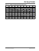
TABLE 12-11: SUMMARY OF REGISTERS ASSOCIATED WITH PORTD
(1)
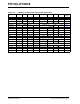
REGISTER 12-16: LATD: PORTD DATA LATCH REGISTER
R/W-x/u R/W-x/u R/W-x/u R/W-x/u R/W-x/u R/W-x/u R/W-x/u R/W-x/u
LATD7 LATD6 LATD5 LATD4 LATD3 LATD2 LATD1 LATD0
bit 7 bit 0
Legend:
R = Readable bit W = Writable bit U = Unimplemented bit, read as ‘0’
u = Bit is unchanged x = Bit is unknown -n/n = Value at POR and BOR/Value at all other Resets
‘1’ = Bit is set ‘0’ = Bit is cleared
bit 7-0 LATD<7:0>: PORTD Output Latch Value bits
(1,2)
Note 1: Writes to PORTD are actually written to corresponding LATD register. Reads from PORTD register is
return of actual I/O pin values.
2: PORTD implemented on PIC16(L)F1939 devices only.
REGISTER 12-17: ANSELD: PORTD ANALOG SELECT REGISTER
(2)
R/W-1/1 R/W-1/1 R/W-1/1 R/W-1/1 R/W-1/1 R/W-1/1 R/W-1/1 R/W-1/1
ANSD7 ANSD6 ANSD5 ANSD4 ANSD3 ANSD2 ANSD1 ANSD0
bit 7 bit 0
Legend:
R = Readable bit W = Writable bit U = Unimplemented bit, read as ‘0’
u = Bit is unchanged x = Bit is unknown -n/n = Value at POR and BOR/Value at all other Resets
‘1’ = Bit is set ‘0’ = Bit is cleared
bit 7-0 ANSD<7:0>: Analog Select between Analog or Digital Function on Pins RD<7:0>, respectively
0 = Digital I/O. Pin is assigned to port or digital special function.
1 = Analog input. Pin is assigned as analog input
(1)
. Digital input buffer disabled.
Note 1: When setting a pin to an analog input, the corresponding TRIS bit must be set to Input mode in order to
allow external control of the voltage on the pin.
2: ANSELD register is not implemented on the PIC16(L)F1938. Read as ‘0’.
3: PORTD implemented on PIC16(L)F1939 devices only.
Name Bit 7 Bit 6 Bit 5 Bit 4 Bit 3 Bit 2 Bit 1 Bit 0
Register on
Page
ANSELD ANSD7 ANSD6 ANSD5 ANSD4 ANSD3 ANSD2 ANSD1 ANSD0 138
CCPxCON
PxM<1:0> DCxB<1:0> CCPxM<3:0> 228
CPSCON0 CPSON CPSRM
— — CPSRNG<1:0> CPSOUT T0XCS 321
CPSCON1
— — — — CPSCH<3:0> 322
LATD LATD7 LATD6 LATD5 LATD4 LATD3 LATD2 LATD1 LATD0 138
LCDCON LCDEN
SLPEN WERR — CS<1:0> LMUX<1:0>
327
LCDSE2
SE23 SE22 SE21 SE20 SE19 SE18 SE17 SE16 331
PORTD RD7 RD6 RD5 RD4 RD3 RD2 RD1 RD0 137
TRISD TRISD7 TRISD6 TRISD5 TRISD4 TRISD3 TRISD2 TRISD1 TRISD0 137
Legend: x = unknown, u = unchanged, – = unimplemented locations read as ‘0’. Shaded cells are not used by PORTD.
Note 1: These registers are not implemented on the PIC16(L)F1938 devices, read as ‘0’.