
Information

PIC16(L)F1824/1828
DS80510H-page 4 2010-2012 Microchip Technology Inc.
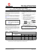
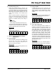
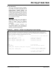
In Figure 1, 88 instruction cycles (TCY) will be
required to complete the full conversion. Each T
AD
cycle consists of 8 TCY periods. A fixed delay is
provided to stop the A/D conversion after 86
instruction cycles and terminate the conversion at
the correct time as shown in the figure above.
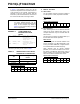
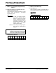
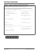
EXAMPLE 1: CODE EXAMPLE OF
INSTRUCTION CYCLE
DELAY
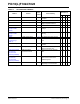
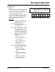
For other combinations of FOSC, TAD values and
Instruction cycle delay counts, refer to Tabl e 3.
TABLE 3: INSTRUCTION CYCLE DELAY
COUNTS BY T
AD SELECTION
Affected Silicon Revisions
2. Module: Oscillator
2.1 HS Oscillator
The HS oscillator requires a minimum voltage of
3.0 volts (at 65°C or less) to operate at 20 MHz.
Work around
None.
Affected Silicon Revisions
2.2 Clock Switching
When switching clock sources between INTOSC
clock source and an external clock source, one
corrupted instruction may be executed after the
switch occurs.
This issue does not affect Two-Speed Start-up or
the Fail-Safe Clock Monitor operation.
Work around
When switching from an external oscillator clock
source, first switch to 16 MHz HFINTOSC. Once
running at 16 MHz HFINTOSC, configure IRCF to
run at desired internal oscillator frequency.
When switching from an internal oscillator
(INTOSC) to an external oscillator clock source,
first switch to HFINTOSC High-Power mode (8
MHz or 16 MHz). Once running from HFINTOSC,
switch to the external oscillator clock source.
Affected Silicon Revisions
Note: The exact delay time will depend on the
T
AD divisor (ADCS) selection. The TCY
counts shown in the timing diagram above
apply to this example only. Refer to
Table 3 for the required delay counts for
other configurations.
TAD
Instruction Cycle Delay
Counts
FOSC/64 172
F
OSC/32 86
FOSC/16 43
A1 A3 A4 A5
X
BSF ADCON0, ADGO ; Start ADC conversion
; Provide 86
instruction cycle
delay here
BCF ADCON0, ADGO ; Terminate the
conversion manually
MOVF ADRESH, W ; Read conversion
result
A1 A3 A4 A5
X
A1 A3 A4 A5
XX