
Information
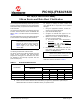

2010-2012 Microchip Technology Inc. DS80510H-page 3
PIC16(L)F1824/1828
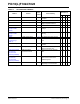
Silicon Errata Issues
1. Module: ADC
1.1 Analog-to-Digital Conversion
An ADC conversion may not complete under these
conditions:
1. When F
OSC is greater than 8 MHz and it is the
clock source used for the ADC converter.
2. The ADC is operating from its dedicated internal
FRC oscillator and the device is not in Sleep
mode (any F
OSC frequency).
When this occurs, the ADC Interrupt Flag (ADIF)
does not get set, the GO/DONE bit does not get
cleared, and the conversion result does not get
loaded into the ADRESH and ADRESL result
registers.
Work around
Method 1: Select the system clock, FOSC, as
the ADC clock source and reduce
the FOSC frequency to 8 MHz or
less when performing ADC
conversions.
Method 2: Select the dedicated FRC
oscillator as the ADC conversion
clock source and perform all
conversions with the device in
Sleep.
Method 3: This method is provided if the
application cannot use Sleep
mode and requires continuous
operation at frequencies above 8
MHz. This method requires early
termination of an ADC conver-
sion. Provide a fixed time delay in
software to stop the A-to-D
conversion manually, after all 10
bits are converted, but before the
conversion would complete auto-
matically. The conversion is
stopped by clearing the GO/
DONE
bit in software. The GO/
DONE
bit must be cleared during
the last ½ T
AD cycle, before the
conversion would have com-
pleted automatically. Refer to
Figure 1 for details.
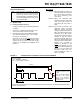
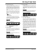
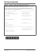
FIGURE 1: INSTRUCTION CYCLE DELAY CALCULATION EXAMPLE
Note: This document summarizes all silicon
errata issues from all revisions of silicon,
previous as well as current. Only the
issues indicated by the shaded column in
the following tables apply to the current
silicon revision (A5).
FOSC = 32 MHz
TCY = 4/32 MHz = 125 nsec
TAD = 1 µsec, ADCS = FOSC/32
88 TCY
84 TCY
8 TCY
4 TCY
1 TAD
11 TAD
Stop the A/D conversion
between 10.5 and 11 T
AD
cycles.
See the Analog-to-Digital
Conversion T
AD Cycles
figure in the Analog-to-
Digital Converter section of
the data sheet.
}
See the ADC Clock Period (T
AD) vs. Device Operating Frequencies table, in the Analog-to-Digital Converter
section of the data sheet.