
Information

PIC16(L)F1826/1827
DS80000485L-page 6 2009-2013 Microchip Technology Inc.
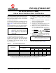
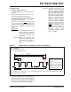
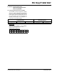
EXAMPLE 1: CODE EXAMPLE OF
INSTRUCTION CYCLE
DELAY
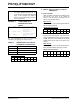
For other combinations of FOSC, TAD values and
Instruction cycle delay counts, refer to Tab l e 3 .
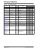
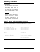
TABLE 3: INSTRUCTION CYCLE DELAY
COUNTS BY T
AD SELECTION
Affected Silicon Revisions
6. Module: Enhanced Capture Compare
PWM (ECCP)
6.1 Enhanced PWM
When the PWM is configured for Full-Bridge mode
and the duty cycle is set to 0%, writing the
PxM<1:0> bits to change the direction has no
effect on PxA and PxC outputs.
Work around
Increase the duty cycle to a value greater than 0%
before changing directions.
Affected Silicon Revisions
6.2 Enhanced PWM
In PWM mode, when the duty cycle is set to 0%
and the STRxSYNC bit is set, writing the STRxA,
STRxB, STRxC and the STRxD bits to enable/
disable steering to port pins has no effect on the
outputs.
Work around
Increase the duty cycle to a value greater than 0%
before enabling/disabling steering to port pins.
Affected Silicon Revisions
Note: The exact delay time will depend on the
T
AD divisor (ADCS) selection. The TCY
counts shown in the timing diagram above
apply to this example only. Refer to
Table 3 for the required delay counts for
other configurations.
T
AD Instruction Cycle Delay Counts
F
OSC/64 172
FOSC/32 86
FOSC/16 43
A2 A3 A4 A5 A6
X X
BSF ADCON0, ADGO ; Start ADC conversion
; Provide 86
instruction cycle
delay here
BCF ADCON0, ADGO ; Terminate the
conversion manually
MOVF ADRESH, W ; Read conversion
result
A2 A3 A4 A5 A6
X X
A2 A3 A4 A5 A6
X X