
Datasheet


2011 Microchip Technology Inc. DS41391D-page 211
PIC16(L)F1826/27
24.3.7 OPERATION IN SLEEP MODE
In Sleep mode, the TMRx register will not increment
and the state of the module will not change. If the CCPx
pin is driving a value, it will continue to drive that value.
When the device wakes up, TMRx will continue from its
previous state.
24.3.8 CHANGES IN SYSTEM CLOCK
FREQUENCY
The PWM frequency is derived from the system clock
frequency. Any changes in the system clock frequency
will result in changes to the PWM frequency. See
Section 5.0 “Oscillator Module (With Fail-Safe
Clock Monitor)” for additional details.
24.3.9 EFFECTS OF RESET
Any Reset will force all ports to Input mode and the
CCP registers to their Reset states.
24.3.10 ALTERNATE PIN LOCATIONS
This module incorporates I/O pins that can be moved to
other locations with the use of the alternate pin function
registers, APFCON0 and APFCON1. To determine
which pins can be moved and what their default loca-
tions are upon a reset, see Section 12.1 “Alternate
Pin Function” for more information.
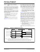
TABLE 24-8: SUMMARY OF REGISTERS ASSOCIATED WITH STANDARD PWM
Name Bit 7 Bit 6 Bit 5 Bit 4 Bit 3 Bit 2 Bit 1 Bit 0
Register
on Page
APFCON0
RXDTSEL SDO1SEL SS1SEL P2BSEL
(2)
CCP2SEL
(2)
P1DSEL P1CSEL CCP1SEL
119
CCPxCON PxM1
(1)
PxM0
(1)
DCxB1 DCxB0 CCPxM3 CCPxM2 CCPxM1 CCPxM0 226
CCPxAS CCPxASE CCPxAS2 CCPxAS1 CCPxAS0 PSSxAC1 PSSxAC0 PSSxBD1 PSSxBD0 228
CCPTMRS C4TSEL1 C4TSEL0 C3TSEL1 C3TSEL0 C2TSEL1 C2TSEL0 C1TSEL1 C1TSEL0 227
INTCON GIE PEIE
TMR0IE INTE IOCIE TMR0IF INTF IOCIF
86
PR2
Timer2 Period Register
189*
PR4 Timer4 Module Period Register
189*
PR6 Timer6 Module Period Register
189*
PSTRxCON
— — — STRxSYNC STRxD STRxC STRxB STRxA 230
PWMxCON PxRSEN PxDC6 PxDC5 PxDC4 PxDC3 PxDC2 PxDC1 PxDC0 229
T2CON
— T2OUTPS3 T2OUTPS2 T2OUTPS1 T2OUTPS0 TMR2ON T2CKPS1 T2CKPS0
191
T4CON
— T4OUTPS3 T4OUTPS2 T4OUTPS1 T4OUTPS0 TMR4ON T4CKPS1 T4CKPS0
191
T6CON
— T6OUTPS3 T6OUTPS2 T6OUTPS1 T6OUTPS0 TMR6ON T6CKPS1 T6CKPS0
191
TMR2 Holding Register for the 8-bit TMR2 Time Base
189*
TMR4 Holding Register for the 8-bit TMR4 Time Base
(1)
189*
TMR6 Holding Register for the 8-bit TMR6 Time Base
(1)
189*
TRISB
TRISB7 TRISB6 TRISB5 TRISB4 TRISB3 TRISB2 TRISB1 TRISB0 127
Legend: — = Unimplemented locations, read as ‘0’. Shaded cells are not used by the PWM.
* Page provides register information.
Note 1: Applies to ECCP modules only.
2: PIC16(L)F1827 only.