
Datasheet


2011 Microchip Technology Inc. DS41391D-page 207
PIC16(L)F1826/27
24.2.5 COMPARE DURING SLEEP
The Compare mode is dependent upon the system
clock (F
OSC) for proper operation. Since FOSC is shut
down during Sleep mode, the Compare mode will not
function properly during Sleep.
24.2.6 ALTERNATE PIN LOCATIONS
This module incorporates I/O pins that can be moved to
other locations with the use of the alternate pin function
registers, APFCON0 and APFCON1. To determine
which pins can be moved and what their default loca-
tions are upon a reset, see Section 12.1 “Alternate
Pin Function” for more information.
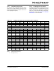
TABLE 24-4: SUMMARY OF REGISTERS ASSOCIATED WITH COMPARE
Name Bit 7 Bit 6 Bit 5 Bit 4 Bit 3 Bit 2 Bit 1 Bit 0
Register
on Page
APFCON0
RXDTSEL SDO1SEL SS1SEL P2BSEL
(2)
CCP2SEL
(2)
P1DSEL P1CSEL CCP1SEL
119
CCPxCON PxM1
(1)
PxM0
(1)
DCxB1 DCxB0 CCPxM3 CCPxM2 CCPxM1 CCPxM0
226
CCPRxL Capture/Compare/PWM Register x Low Byte (LSB)
204*
CCPRxH Capture/Compare/PWM Register x High Byte (MSB)
204*
CM1CON0 C1ON C1OUT C1OE C1POL
— C1SP C1HYS C1SYNC
170
CM1CON1 C1INTP C1INTN C1PCH1 C1PCH0
— — C1NCH1 C1NCH0
171
CM2CON0 C2ON C2OUT C2OE C2POL
— C2SP C2HYS C2SYNC
170
CM2CON1 C2INTP C2INTN C2PCH1 C2PCH0
— — C2NCH1 C2NCH0
171
INTCON GIE PEIE
TMR0IE INTE IOCIE TMR0IF INTF IOCIF
86
PIE1 TMR1GIE
ADIE RCIE TXIE SSPIE CCP1IE TMR2IE TMR1IE
87
PIE2
OSFIE C2IE C1IE EEIE BCL1IE — — CCP2IE
(2)
88
PIE3
(2)
—
—
CCP4IE CCP3IE TMR6IE
—TMR4IE—
89
PIR1 TMR1GIF
ADIF RCIF TXIF SSPIF CCP1IF TMR2IF TMR1IF
91
PIR2
OSFIF C2IF C1IF EEIF BCLIF — —CCP2IF
(2)
92
PIR3
(2)
—
—
CCP4IF CCP3IF
TMR6IF — TMR4IF —
93
T1CON TMR1CS1 TMR1CS0 T1CKPS1 T1CKPS0 T1OSCEN T1SYNC
—TMR1ON
185
T1GCON TMR1GE T1GPOL T1GTM T1GSPM T1GGO/DONE T1GVAL T1GSS1 T1GSS0
186
TMR1L Holding Register for the Least Significant Byte of the 16-bit TMR1 Register
177*
TMR1H Holding Register for the Most Significant Byte of the 16-bit TMR1 Register
177*
TRISA
TRISA7 TRISA6 TRISA5 TRISA4 TRISA3 TRISA2 TRISA1 TRISA0
122
TRISB
TRISB7 TRISB6 TRISB5 TRISB4 TRISB3 TRISB2 TRISB1 TRISB0
127
Legend: — = Unimplemented locations, read as ‘0’. Shaded cells are not used by Compare mode.
* Page provides register information.
Note 1: Applies to ECCP modules only.
2: PIC16(L)F1827 only.