
Datasheet


2011 Microchip Technology Inc. DS41391D-page 137
PIC16(L)F1826/27
15.0 TEMPERATURE INDICATOR
MODULE
This family of devices is equipped with a temperature
circuit designed to measure the operating temperature
of the silicon die. The circuit's range of operating
temperature falls between of -40°C and +85°C. The
output is a voltage that is proportional to the device
temperature. The output of the temperature indicator is
internally connected to the device ADC.
The circuit may be used as a temperature threshold
detector or a more accurate temperature indicator,
depending on the level of calibration performed. A one-
point calibration allows the circuit to indicate a
temperature closely surrounding that point. A two-point
calibration allows the circuit to sense the entire range
of temperature more accurately. Reference Application
Note AN1333, “Use and Calibration of the Internal
Temperature Indicator” (DS01333) for more details
regarding the calibration process.
15.1 Circuit Operation
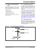
Figure 15-1 shows a simplified block diagram of the
temperature circuit. The proportional voltage output is
achieved by measuring the forward voltage drop across
multiple silicon junctions.
Equation 15-1 describes the output characteristics of
the temperature indicator.
EQUATION 15-1: VOUT RANGES
The temperature sense circuit is integrated with the
Fixed Voltage Reference (FVR) module. See
Section 14.0 “Fixed Voltage Reference (FVR)” for
more information.
The circuit is enabled by setting the TSEN bit of the
FVRCON register. When disabled, the circuit draws no
current.
The circuit operates in either high or low range. The high
range, selected by setting the TSRNG bit of the
FVRCON register, provides a wider output voltage. This
provides more resolution over the temperature range,
but may be less consistent from part to part. This range
requires a higher bias voltage to operate and thus, a
higher V
DD is needed.
The low range is selected by clearing the TSRNG bit of
the FVRCON register. The low range generates a lower
voltage drop and thus, a lower bias voltage is needed to
operate the circuit. The low range is provided for low
voltage operation.
FIGURE 15-1: TEMPERATURE CIRCUIT
DIAGRAM
15.2 Minimum Operating VDD vs.
Minimum Sensing Temperature
When the temperature circuit is operated in low range,
the device may be operated at any operating voltage
that is within specifications.
When the temperature circuit is operated in high range,
the device operating voltage, V
DD, must be high
enough to ensure that the temperature circuit is cor-
rectly biased.
Table 15-1 shows the recommended minimum V
DD vs.
range setting.
TABLE 15-1: RECOMMENDED VDD VS.
RANGE
15.3 Temperature Output
The output of the circuit is measured using the internal
analog to digital converter. Channel 29 is reserved for
the temperature circuit output. Refer to Section 16.0
“Analog-to-Digital Converter (ADC) Module” for
detailed information.
High Range: VOUT = VDD - 4VT
Low Range: VOUT = VDD - 2VT
Min. VDD, TSRNG = 1 Min. VDD, TSRNG = 0
3.6V 1.8V
TSEN
ADC
MUX
TSRNG
VDD
ADC
CHS bits
(ADCON0 register)
n
V
OUT