
Information

PIC16(L)F1825/1829
DS80000517E-page 4 2011-2013 Microchip Technology Inc.
2. Module: Timer1
2.1 Timer1 Gate Toggle mode
When Timer1 Gate Toggle mode is enabled, it is
possible to measure the full-cycle length of a
Timer1 gate signal. To perform this function, the
Timer1 gate source is routed through a flip-flop
that changes state on every incrementing edge of
the gate signal. Timer1 Gate Toggle mode is
enabled by setting the T1GTM bit of the T1GCON
register. When working properly, clearing either
the T1GTM bit or the TMR1ON bit would also clear
the output value of this flip-flop, and hold it clear.
This is done in order to control which edge is being
measured. The issue that exists is that clearing the
TMR1ON bit does not clear the output value of the
flip-flop and hold it clear.
Work around
Clear the T1GTM bit in the T1GCON register to
clear and hold clear the output value of the flip-flop.
Affected Silicon Revisions
3. Module: ADC
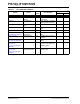
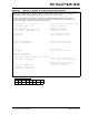
3.1 ADC Differential and Gain Error Parameters
The differential and gain error parameters are as
follows:
Work around
None.
Affected Silicon Revisions
A0 A2
X
Param
No.
Sym. Characteristic Min. Typ† Max. Units Conditions
AD03 EDL Differential Error — — ±1.5 LSb VREF = 3.0V. Missing codes = 2
AD04 E
OFF Offset Error — — ±2 LSb VREF = 3.0V. At -40°C offset is ±3
AD05 EGN Gain Error — — ±2 LSb VREF = 3.0V
A0 A2
X
X