
Datasheet


2010-2012 Microchip Technology Inc. DS41419D-page 211
PIC16(L)F1824/1828
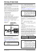
REGISTER 23-2: MDSRC: MODULATION SOURCE CONTROL REGISTER
R/W-x/u U-0 U-0 U-0 R/W-x/u R/W-x/u R/W-x/u R/W-x/u
MDMSODIS — — —MDMS<3:0>
bit 7 bit 0
Legend:
R = Readable bit W = Writable bit U = Unimplemented bit, read as ‘0’
u = Bit is unchanged x = Bit is unknown -n/n = Value at POR and BOR/Value at all other Resets
‘1’ = Bit is set ‘0’ = Bit is cleared
bit 7 MDMSODIS: Modulation Source Output Disable
1 = Output signal driving the peripheral output pin (selected by MDMS<3:0>) is disabled
0 = Output signal driving the peripheral output pin (selected by MDMS<3:0>) is enabled
bit 6-4 Unimplemented: Read as ‘0’
bit 3-0 MDMS<3:0> Modulation Source Selection bits
1111 = Reserved. No channel connected.
1110 = Reserved. No channel connected.
1101 = Reserved. No channel connected.
1100 = Reserved. No channel connected.
1011 = Reserved. No channel connected.
1010 = EUSART TX output
1001 = MSSP2 SDOx output
1000 = MSSP1 SDOx output
0111 = Comparator2 output
0110 = Comparator1 output
0101 = CCP4 output (PWM Output mode only)
0100 = CCP3 output (PWM Output mode only)
0011 = CCP2 output (PWM Output mode only)
0010 = CCP1 output (PWM Output mode only)
0001 = MDMIN port pin
0000 = MDBIT bit of MDCON register is modulation source
Note 1: Narrowed carrier pulse widths or spurs may occur in the signal stream if the carrier is not synchronized.