
Datasheet


2010-2012 Microchip Technology Inc. DS41419D-page 139
PIC16(L)F1824/1828
TABLE 12-4: SUMMARY OF REGISTERS ASSOCIATED WITH PORTC
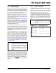
REGISTER 12-20: INLVLC: PORTC INPUT LEVEL CONTROL REGISTER
U-0
(3)
R/W-1/1
(2)
U-0
(3)
R/W-1/1
(2)
R/W-0/0
(3)
R/W-1/1
(2)
R/W-0/0
(3)
R/W-1/1
(2)
R/W-0/0
(3)
R/W-1/1
(2)
R/W-0/0
(3)
R/W-1/1
(2)
R/W-0/0
(3)
R/W-1/1
(2)
R/W-0/0
(3)
R/W-1/1
(2)
INLVLC7
(1)
INLVLC6
(1)
INLVLC5 INLVLC4 INLVLC3 INLVLC2 INLVLC1 INLVLC0
bit 7 bit 0
Legend:
R = Readable bit W = Writable bit U = Unimplemented bit, read as ‘0’
u = Bit is unchanged x = Bit is unknown -n/n = Value at POR and BOR/Value at all other Resets
‘1’ = Bit is set ‘0’ = Bit is cleared
bit 7-0 INLVLC<7:0>: PORTC Input Level Select bits
(1)
For RC<7:0> pins, respectively
1 = ST input used for PORT reads and Interrupt-on-Change
0 = TTL input used for PORT reads and Interrupt-on-Change
Note 1: INLVLC<7:6> available on PIC16(L)F1828 only. Otherwise, they are unimplemented and read as ‘0’.
2: PIC16(L)F1828 only, Reset default value.
3: PIC16(L)F1824 only, Reset default value.
Name Bit 7 Bit 6 Bit 5 Bit 4 Bit 3 Bit 2 Bit 1 Bit 0
Register
on Page
ANSELC ANSC7
(1)
ANSC6
(1)
— — ANSC3 ANSC2 ANSC1 ANSC0 138
INLVLC INLVLC7
(1)
INLVLC6
(1)
INLVLC5 INLVLC4 INLVLC3 INLVLC2 INLVLC1 INLVLC0 139
LATC LATC7
(1)
LATC6
(1)
LATC5 LATC4 LATC3 LATC2 LATC1 LATC0 137
PORTC RC7
(1)
RC6
(1)
RC5 RC4 RC3 RC2 RC1 RC0 137
TRISC TRISC7
(1)
TRISC6
(1)
TRISC5 TRISC4 TRISC3 TRISC2 TRISC1 TRISC0 137
WPUC WPUC7
(1)
WPUC6
(1)
WPUC5 WPUC4 WPUC3 WPUC2 WPUC1 WPUC0
138
Legend: x = unknown, u = unchanged, - = unimplemented locations, read as ‘0’. Shaded cells are not used by PORTC.
Note 1: PIC16(L)F1828 only.