
Datasheet


2011-2012 Microchip Technology Inc. Preliminary DS41579D-page 109
PIC16(L)F1782/3
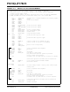
FIGURE 12-2: BLOCK WRITES TO FLASH PROGRAM MEMORY WITH 32 WRITE LATCHES
EXAMPLE 12-4: ERASING ONE ROW OF PROGRAM MEMORY
14
14 14 14
Program Memory
Buffer Register
EEADRL<4:0> = 00000
Buffer Register
EEADRL<4:0> = 00001
Buffer Register
EEADRL<4:0> = 00010
Buffer Register
EEADRL<4:0> = 11111
EEDATAEEDATH
75
07
0
6
8
First word of block
to be written
Last word of block
to be written
; This row erase routine assumes the following:
; 1. A valid address within the erase block is loaded in ADDRH:ADDRL
; 2. ADDRH and ADDRL are located in shared data memory 0x70 - 0x7F (common RAM)
BCF INTCON,GIE ; Disable ints so required sequences will execute properly
BANKSEL EEADRL
MOVF ADDRL,W ; Load lower 8 bits of erase address boundary
MOVWF EEADRL
MOVF ADDRH,W ; Load upper 6 bits of erase address boundary
MOVWF EEADRH
BSF EECON1,EEPGD ; Point to program memory
BCF EECON1,CFGS ; Not configuration space
BSF EECON1,FREE ; Specify an erase operation
BSF EECON1,WREN ; Enable writes
MOVLW 55h ; Start of required sequence to initiate erase
MOVWF EECON2 ; Write 55h
MOVLW 0AAh ;
MOVWF EECON2 ; Write AAh
BSF EECON1,WR ; Set WR bit to begin erase
NOP ; Any instructions here are ignored as processor
; halts to begin erase sequence
NOP ; Processor will stop here and wait for erase complete.
; after erase processor continues with 3rd instruction
BCF EECON1,WREN ; Disable writes
BSF INTCON,GIE ; Enable interrupts
Required
Sequence