
Datasheet


Table Of Contents
- High-Performance RISC CPU:
- Flexible Oscillator Structure:
- Special Microcontroller Features:
- Extreme Low-Power Management PIC16LF1526/7 with XLP:
- Analog Features:
- Peripheral Features:
- PIC16(L)F151X/152X Family Types
- Table of Contents
- Most Current Data Sheet
- Errata
- Customer Notification System
- 1.0 Device Overview
- 2.0 Enhanced Mid-Range CPU
- 3.0 Memory Organization
- 4.0 Device Configuration
- 5.0 Oscillator Module (with Fail-Safe Clock Monitor)
- 6.0 Resets
- FIGURE 6-1: Simplified Block Diagram of On-Chip Reset Circuit
- 6.1 Power-On Reset (POR)
- 6.2 Brown-Out Reset (BOR)
- 6.3 Register Definitions: BOR Control
- 6.4 Low-Power Brown-Out Reset (LPBOR)
- 6.5 MCLR
- 6.6 Watchdog Timer (WDT) Reset
- 6.7 RESET Instruction
- 6.8 Stack Overflow/Underflow Reset
- 6.9 Programming Mode Exit
- 6.10 Power-up Timer
- 6.11 Start-up Sequence
- 6.12 Determining the Cause of a Reset
- 6.13 Power Control (PCON) Register
- 6.14 Register Definitions: Power Control
- 7.0 Interrupts
- FIGURE 7-1: Interrupt Logic
- 7.1 Operation
- 7.2 Interrupt Latency
- 7.3 Interrupts During Sleep
- 7.4 INT Pin
- 7.5 Automatic Context Saving
- 7.6 Register Definitions: Interrupt Control
- Register 7-1: INTCON: Interrupt Control Register
- Register 7-2: PIE1: Peripheral Interrupt Enable Register 1
- Register 7-3: PIE2: Peripheral Interrupt Enable Register 2
- Register 7-4: PIE3: Peripheral Interrupt Enable Register 3
- Register 7-5: PIE4: Peripheral Interrupt Enable Register 4
- Register 7-6: PIR1: Peripheral Interrupt Request Register 1
- Register 7-7: PIR2: Peripheral Interrupt Request Register 2
- Register 7-8: PIR3: Peripheral Interrupt Request Register 3
- Register 7-9: PIR4: Peripheral Interrupt Request Register 4
- TABLE 7-1: Summary of Registers Associated with Interrupts
- 8.0 Power-Down Mode (Sleep)
- 9.0 Low Dropout (LDO) Voltage Regulator
- 10.0 Watchdog Timer (WDT)
- 11.0 Flash Program Memory Control
- 11.1 PMADRL and PMADRH Registers
- 11.2 Flash Program Memory Overview
- 11.3 Modifying Flash Program Memory
- 11.4 User ID, Device ID and Configuration Word Access
- 11.5 Write Verify
- 11.6 Register Definitions: Flash Program Memory Control
- Register 11-1: PMDATL: Program Memory Data Low Byte Register
- Register 11-2: PMDATH: Program Memory Data High Byte Register
- Register 11-3: PMADRL: Program Memory Address Low Byte Register
- Register 11-4: PMADRH: Program Memory Address High Byte Register
- Register 11-5: PMCON1: Program Memory Control 1 Register
- Register 11-6: PMCON2: Program Memory Control 2 Register
- TABLE 11-3: Summary of Registers Associated with Flash Program Memory
- TABLE 11-4: Summary of Configuration Word with Flash Program Memory
- 12.0 I/O Ports
- TABLE 12-1: Port Availability per Device
- FIGURE 12-1: Generic I/O Port Operation
- 12.1 Alternate Pin Function
- 12.2 Register Definitions: Alternate Pin Function Control
- 12.3 PORTA Registers
- 12.4 Register Definitions: PORTA
- 12.5 PORTB Registers
- 12.6 Register Definitions: PORTB
- 12.7 PORTC Registers
- 12.8 Register Definitions: PORTC
- 12.9 PORTD Registers
- 12.10 Register Definitions: PORTD
- 12.11 PORTE Registers
- 12.12 Register Definitions: PORTE
- 12.13 PORTF Registers
- 12.14 Register Definitions: PORTF
- 12.15 PORTG Registers
- 12.16 Register Definitions: PORTG
- Register 12-28: PORTG: PORTG Register
- Register 12-29: TRISG: PORTG Tri-State Register
- Register 12-30: LATG: PORTG Data Latch Register
- Register 12-31: ANSELG: PORTG Analog Select Register
- Register 12-32: WPUG: Weak Pull-up PORTG Register
- TABLE 12-17: Summary of Registers Associated with PORTG
- TABLE 12-18: Summary of cONFIGURATION wORD with PORTG
- 13.0 Interrupt-On-Change
- 14.0 Fixed Voltage Reference (FVR)
- 15.0 Temperature Indicator Module
- 16.0 Analog-to-Digital Converter (ADC) Module
- FIGURE 16-1: ADC Block Diagram
- 16.1 ADC Configuration
- 16.2 ADC Operation
- 16.3 Register Definitions: ADC Control
- Register 16-1: ADCON0: ADC Control Register 0
- Register 16-2: ADCON1: ADC Control Register 1
- Register 16-3: ADRESH: ADC Result Register High (ADRESH) ADFM = 0
- Register 16-4: ADRESL: ADC Result Register Low (ADRESL) ADFM = 0
- Register 16-5: ADRESH: ADC Result Register High (ADRESH) ADFM = 1
- Register 16-6: ADRESL: ADC Result Register Low (ADRESL) ADFM = 1
- 16.4 ADC Acquisition Requirements
- 17.0 Timer0 Module
- 18.0 Timer1/3/5 Module with Gate Control
- FIGURE 18-1: Timer1/3/5 Block Diagram
- FIGURE 18-2: Timer1/3/5 Clock Source Diagram
- 18.1 Timer1/3/5 Operation
- 18.2 Clock Source Selection
- 18.3 Timer1/3/5 Prescaler
- 18.4 Timer1/3/5 Oscillator
- 18.5 Timer1/3/5 Operation in Asynchronous Counter Mode
- 18.6 Timer1/3/5 Gate
- 18.7 Timer1/3/5 Interrupt
- 18.8 Timer1/3/5 Operation During Sleep
- 18.9 ECCP/CCP Capture/Compare Time Base
- 18.10 ECCP/CCP Special Event Trigger
- 18.11 Register Definitions: Timer1/3/5 Control
- 18.12 Register Definitions: Timer1/3/5 Gate Control
- 19.0 Timer2/4/6/8/10 Modules
- 20.0 Capture/Compare/PWM Modules
- 20.1 Capture Mode
- 20.2 Compare Mode
- 20.3 PWM Overview
- 20.4 Register Definitions: ECCP Control
- 21.0 Master Synchronous Serial Port (MSSP1 and MSSP2) Module
- 21.1 Master SSPx (MSSPx) Module Overview
- 21.2 SPI Mode Overview
- 21.3 I2C Mode Overview
- 21.4 I2C Mode Operation
- 21.5 I2C Slave Mode Operation
- 21.5.1 Slave Mode Addresses
- 21.5.2 Slave Reception
- FIGURE 21-14: I2C Slave, 7-bit Address, Reception (SEN = 0, AHEN = 0, DHEN = 0)
- FIGURE 21-15: I2C Slave, 7-bit Address, Reception (SEN = 1, AHEN = 0, DHEN = 0)
- FIGURE 21-16: I2C Slave, 7-bit Address, Reception (SEN = 0, AHEN = 1, DHEN = 1)
- FIGURE 21-17: I2C Slave, 7-bit Address, Reception (SEN = 1, AHEN = 1, DHEN = 1)
- 21.5.3 Slave Transmission
- 21.5.4 Slave Mode 10-bit Address Reception
- 21.5.5 10-bit Addressing with Address or Data Hold
- 21.5.6 Clock Stretching
- 21.5.7 Clock Synchronization and the CKP bit
- 21.5.8 General Call Address Support
- 21.5.9 SSPx Mask Register
- 21.6 I2C Master Mode
- 21.6.1 I2C Master Mode Operation
- 21.6.2 Clock Arbitration
- 21.6.3 WCOL Status Flag
- 21.6.4 I2C Master Mode Start Condition Timing
- 21.6.5 I2C Master Mode Repeated Start Condition Timing
- 21.6.6 I2C Master Mode Transmission
- 21.6.7 I2C Master Mode Reception
- 21.6.8 Acknowledge Sequence Timing
- 21.6.9 Stop Condition Timing
- 21.6.10 Sleep Operation
- 21.6.11 Effects of a Reset
- 21.6.12 Multi-Master Mode
- 21.6.13 Multi -Master Communication, Bus Collision and Bus Arbitration
- FIGURE 21-32: Bus Collision Timing for Transmit and Acknowledge
- FIGURE 21-33: Bus Collision During Start Condition (SDAx Only)
- FIGURE 21-34: Bus Collision During Start Condition (SCLx = 0)
- FIGURE 21-35: BRG Reset Due to Sda Arbitration During Start Condition
- FIGURE 21-36: Bus Collision During a Repeated Start Condition (Case 1)
- FIGURE 21-37: Bus Collision During Repeated Start Condition (Case 2)
- FIGURE 21-38: Bus Collision During a Stop Condition (Case 1)
- FIGURE 21-39: Bus Collision During a Stop Condition (Case 2)
- TABLE 21-3: Summary of Registers Associated with I2C™ Operation
- 21.7 Baud Rate Generator
- 21.8 Register Definitions: MSSP Control
- Register 21-1: SSPxSTAT: SSPx Status Register
- Register 21-2: SSPxCON1: SSPx Control Register 1
- Register 21-3: SSPxCON2: SSPx Control Register 2
- Register 21-4: SSPxCON3: SSPx Control Register 3
- Register 21-5: SSPxMSK: SSPx Mask Register
- Register 21-6: SSPxADD: MSSPx Address and Baud Rate Register (I2C Mode)
- 22.0 Enhanced Universal Synchronous Asynchronous Receiver Transmitter (EUSART)
- FIGURE 22-1: EUSART Transmit Block Diagram
- FIGURE 22-2: EUSART Receive Block Diagram
- 22.1 EUSART Asynchronous Mode
- 22.2 Clock Accuracy with Asynchronous Operation
- 22.3 Register Definitions: EUSART Control
- 22.4 EUSART Baud Rate Generator (BRG)
- EXAMPLE 22-1: Calculating Baud Rate Error
- TABLE 22-3: Baud Rate Formulas
- TABLE 22-4: Summary of Registers Associated with the Baud Rate Generator
- TABLE 22-5: Baud Rates for Asynchronous Modes
- 22.4.1 Auto-Baud Detect
- 22.4.2 Auto-Baud Overflow
- 22.4.3 Auto-Wake-up on Break
- 22.4.4 Break Character Sequence
- 22.4.5 Receiving a Break Character
- 22.5 EUSART Synchronous Mode
- 22.5.1 Synchronous Master Mode
- FIGURE 22-10: Synchronous Transmission
- FIGURE 22-11: Synchronous Transmission (through TXEN)
- TABLE 22-7: Summary of Registers Associated with Synchronous Master Transmission
- FIGURE 22-12: Synchronous Reception (Master Mode, SREN)
- TABLE 22-8: Summary of Registers Associated with Synchronous Master Reception
- 22.5.2 Synchronous Slave Mode
- 22.5.1 Synchronous Master Mode
- 23.0 In-Circuit Serial Programming™ (ICSP™)
- 24.0 Instruction Set Summary
- 25.0 Electrical Specifications
- Absolute Maximum Ratings(†)
- 25.1 DC Characteristics: Supply Voltage
- 25.2 DC Characteristics: Supply Current (Idd)
- 25.3 DC Characteristics: Power-Down Currents (Ipd)
- 25.4 DC Characteristics: I/O Ports
- 25.5 Memory Programming Requirements
- 25.6 Thermal Considerations
- 25.7 Timing Parameter Symbology
- 25.8 AC Characteristics: PIC16(L)F1526/7-I/E
- FIGURE 25-6: Clock Timing
- TABLE 25-1: Clock Oscillator Timing Requirements
- TABLE 25-2: Oscillator Parameters
- FIGURE 25-7: CLKOUT and I/O Timing
- TABLE 25-3: CLKOUT and I/O Timing Parameters
- FIGURE 25-8: Reset, Watchdog Timer, Oscillator Start-up Timer and Power-up Timer Timing
- FIGURE 25-9: Brown-Out Reset Timing and Characteristics
- TABLE 25-4: Reset, Watchdog Timer, Oscillator Start-up Timer, Power-up Timer and Brown-Out Reset Parameters
- FIGURE 25-10: Timer0 and Timer1 External Clock Timings
- TABLE 25-5: Timer0 and Timer1 External Clock Requirements
- FIGURE 25-11: Capture/Compare/PWM Timings (CCP)
- TABLE 25-6: Capture/Compare/PWM Requirements (CCP)
- TABLE 25-7: Analog-to-Digital Converter (ADC) Characteristics(1,2,3)
- TABLE 25-8: ADC Conversion Requirements
- FIGURE 25-12: ADC Conversion Timing (Normal Mode)
- FIGURE 25-13: ADC Conversion Timing (Sleep Mode)
- TABLE 25-9: Low Dropout (LDO) Regulator Characteristics
- FIGURE 25-14: USART Synchronous Transmission (Master/Slave) Timing
- TABLE 25-10: USART Synchronous Transmission Requirements
- FIGURE 25-15: USART Synchronous Receive (Master/Slave) Timing
- TABLE 25-11: USART Synchronous Receive Requirements
- FIGURE 25-16: SPI Master Mode Timing (CKE = 0, SMP = 0)
- FIGURE 25-17: SPI Master Mode Timing (CKE = 1, SMP = 1)
- FIGURE 25-18: SPI Slave Mode Timing (CKE = 0)
- FIGURE 25-19: SPI Slave Mode Timing (CKE = 1)
- TABLE 25-12: SPI Mode requirements
- FIGURE 25-20: I2C™ Bus Start/Stop Bits Timing
- TABLE 25-13: I2C™ Bus Start/Stop Bits Requirements
- FIGURE 25-21: I2C™ Bus Data Timing
- TABLE 25-14: I2C™ Bus Data Requirements
- 26.0 DC and AC Characteristics Graphs and Charts
- FIGURE 26-1: Idd, LP Oscillator, Fosc = 32 kHz, PIC16LF1526 ONLY
- FIGURE 26-2: Idd, LP Oscillator, Fosc = 32 kHz, PIC16F1526/7 ONLY
- FIGURE 26-3: Idd Typical, XT and EXTRC Oscillator, PIC16LF1526 ONLY
- FIGURE 26-4: Idd Maximum, XT and EXTRC Oscillator, PIC16LF1526 ONLY
- FIGURE 26-5: Idd Typical, XT and EXTRC Oscillator, PIC16F1526/7 ONLY
- FIGURE 26-6: Idd Maximum, XT and EXTRC Oscillator, PIC16F1526/7 ONLY
- FIGURE 26-7: Idd, External Clock (ECL), Low-Power Mode, Fosc = 32 kHz, PIC16LF1526 ONLY
- FIGURE 26-8: Idd, External Clock (ECL), Low-Power Mode, Fosc = 32 kHz, PIC16F1526/7 ONLY
- FIGURE 26-9: Idd, External Clock (ECL), Low-Power Mode, Fosc = 500 kHz, PIC16LF1526 ONLY
- FIGURE 26-10: Idd, External Clock (ECL), Low-Power Mode, Fosc = 500 kHz, PIC16F1526/7 ONLY
- FIGURE 26-11: Idd Typical, External Clock (ECM), Medium-Power Mode, PIC16LF1526 ONLY
- FIGURE 26-12: Idd Maximum, External Clock (ECM), Medium-Power Mode, PIC16LF1526 ONLY
- FIGURE 26-13: Idd Typical, External Clock (ECM), Medium-Power Mode, PIC16F1526/7 ONLY
- FIGURE 26-14: Idd Maximum, External Clock (ECM), Medium-Power Mode, PIC16F1526/7 ONLY
- FIGURE 26-15: Idd Typical, External Clock (ECH), High-Power Mode, PIC16LF1526 ONLY
- FIGURE 26-16: Idd Maximum, External Clock (ECH), High-Power Mode, PIC16LF1526 ONLY
- FIGURE 26-17: Idd Typical, External Clock (ECH), High-Power Mode, PIC16F1526/7 ONLY
- FIGURE 26-18: Idd Maximum, External Clock (ECH), High-Power Mode, PIC16F1526/7 ONLY
- FIGURE 26-19: Idd, LFINTOSC, Fosc = 31 kHz, PIC16LF1526 Only
- FIGURE 26-20: Idd, LFINTOSC, Fosc = 31 kHz, PIC16F1526/7 Only
- FIGURE 26-21: Idd, MFINTOSC, Fosc = 500 kHz, PIC16LF1526 ONLY
- FIGURE 26-22: Idd, MFINTOSC, Fosc = 500 kHz, PIC16F1526/7 ONLY
- FIGURE 26-23: Idd Typical, HFINTOSC, PIC16LF1526 ONLY
- FIGURE 26-24: Idd Maximum, HFINTOSC, PIC16LF1526 ONLY
- FIGURE 26-25: Idd Typical, HFINTOSC, PIC16F1526/7 ONLY
- FIGURE 26-26: Idd Maximum, HFINTOSC, PIC16F1526/7 ONLY
- FIGURE 26-27: Idd Typical, HS OScillator, PIC16LF1526 ONLY
- FIGURE 26-28: Idd Maximum, HS Oscillator, PIC16LF1526 ONLY
- FIGURE 26-29: Idd Typical, HS Oscillator, PIC16F1526/7 ONLY
- FIGURE 26-30: Idd Maximum, HS Oscillator, PIC16F1526/7 ONLY
- FIGURE 26-31: Ipd Base, Sleep Mode, PIC16LF1526 ONly
- FIGURE 26-32: Ipd Base, Low-Power Sleep Mode, VREGPM = 1, PIC16F1526/7 ONLy
- FIGURE 26-33: Ipd, Watchdog Timer (WDT), PIC16LF1526 ONLy
- FIGURE 26-34: Ipd, Watchdog Timer (WDT), PIC16F1526/7 ONLy
- FIGURE 26-35: Ipd, Fixed Voltage Reference (FVR), PIC16LF1526 ONLy
- FIGURE 26-36: Ipd, Fixed Voltage Reference (FVR), PIC16F1526/7 ONLy
- FIGURE 26-37: Ipd, Brown-Out Reset (BOR), BORV = 1, PIC16LF1526 ONLY
- FIGURE 26-38: Ipd, Brown-Out Reset (BOR), BORV = 1, PIC16F1526/7 ONLy
- FIGURE 26-39: Ipd, Secondary Oscillator, Fosc = 32 kHz, PIC16LF1526 ONLy
- FIGURE 26-40: Ipd, Secondary Oscillator, Fosc = 32 kHz, PIC16F1526/7 ONly
- FIGURE 26-41: Voh vs. Ioh over Temperature, Vdd = 5.5V, PIC16F1526/7 ONLy
- FIGURE 26-42: Vol vs. Iol over Temperature, Vdd = 5.5V, PIC16F1526/7 ONLy
- FIGURE 26-43: Voh vs. Ioh over Temperature, Vdd = 3.0V
- FIGURE 26-44: Vol vs. Iol over Temperature, Vdd = 3.0V
- FIGURE 26-45: Voh vs. Ioh over Temperature, Vdd = 1.8V, PIC16LF1526 Only
- FIGURE 26-46: Vol vs. Iol over Temperature, Vdd = 1.8V, PIC16LF1526 Only
- FIGURE 26-47: POR Release Voltage
- FIGURE 26-48: POR Rearm Voltage, PIC16F1526/7 ONLy
- FIGURE 26-49: Brown-Out Reset Voltage, BORV = 1, PIC16LF1526 Only
- FIGURE 26-50: Brown-Out Reset Hysteresis, BORV = 1, PIC16LF1526 Only
- FIGURE 26-51: Brown-Out Reset Voltage, BORV = 1, PIC16F1526/7 Only
- FIGURE 26-52: Brown-Out Reset Hysteresis, BORV = 1, PIC16F1526/7 Only
- FIGURE 26-53: Brown-Out Reset Voltage, BORV = 0
- FIGURE 26-54: Brown-Out Reset Hysteresis, BORV = 0
- FIGURE 26-55: Low-Power Brown-Out Reset Voltage, LPBOR = 0
- FIGURE 26-56: Low-Power Brown-Out Reset Hysteresis, LPBOR = 0
- FIGURE 26-57: WDT Time-Out Period
- FIGURE 26-58: PWRT Period
- FIGURE 26-59: FVR Stabilization Period
- FIGURE 26-60: LFINTOSC Frequency Over Vdd and Temperature, PIC16LF1526 Only
- FIGURE 26-61: LFINTOSC Frequency Over Vdd and Temperature, PIC16F1526/7 Only
- FIGURE 26-62: Sleep Mode, Wake Period with HFINTOSC Source, PIC16LF1526/7 Only
- FIGURE 26-63: Low-Power Sleep Mode, Wake Period with HFINTOSC Source, VREGPM = 1, PIC16F1526/7 Only
- FIGURE 26-64: Sleep Mode, Wake Period with HFINTOSC Source, VREGPM = 0, PIC16F1526/7 Only
- 27.0 Development Support
- 27.1 MPLAB Integrated Development Environment Software
- 27.2 MPLAB C Compilers for Various Device Families
- 27.3 HI-TECH C for Various Device Families
- 27.4 MPASM Assembler
- 27.5 MPLINK Object Linker/ MPLIB Object Librarian
- 27.6 MPLAB Assembler, Linker and Librarian for Various Device Families
- 27.7 MPLAB SIM Software Simulator
- 27.8 MPLAB REAL ICE In-Circuit Emulator System
- 27.9 MPLAB ICD 3 In-Circuit Debugger System
- 27.10 PICkit 3 In-Circuit Debugger/ Programmer and PICkit 3 Debug Express
- 27.11 PICkit 2 Development Programmer/Debugger and PICkit 2 Debug Express
- 27.12 MPLAB PM3 Device Programmer
- 27.13 Demonstration/Development Boards, Evaluation Kits, and Starter Kits
- 28.0 Packaging Information
- Appendix A: Data Sheet Revision History
- INDEX
- The Microchip Web Site
- Customer Change Notification Service
- Customer Support
- Reader Response
- Product Identification System
- Trademarks
- Worldwide Sales
2011-2013 Microchip Technology Inc. DS41458C-page 51
PIC16(L)F1526/7
5.2 Clock Source Types
Clock sources can be classified as external or internal.
External clock sources rely on external circuitry for the
clock source to function. Examples are: oscillator mod-
ules (EC mode), quartz crystal resonators or ceramic
resonators (LP, XT and HS modes) and Resis-
tor-Capacitor (RC) mode circuits.
Internal clock sources are contained within the oscillator
module. The internal oscillator block has two internal
oscillators that are used to generate the internal system
clock sources: the 16 MHz High-Frequency Internal
Oscillator and the 31 kHz Low-Frequency Internal
Oscillator (LFINTOSC).
The system clock can be selected between external or
internal clock sources via the System Clock Select
(SCS) bits in the OSCCON register. See Section 5.3
“Clock Switching” for additional information.
5.2.1 EXTERNAL CLOCK SOURCES
An external clock source can be used as the device
system clock by performing one of the following
actions:
• Program the FOSC<2:0> bits in the Configuration
Words to select an external clock source that will
be used as the default system clock upon a
device Reset.
• Write the SCS<1:0> bits in the OSCCON register
to switch the system clock source to:
- Secondary oscillator during run-time, or
- An external clock source determined by the
value of the FOSC bits.
See Section 5.3 “Clock Switching”for more informa-
tion.
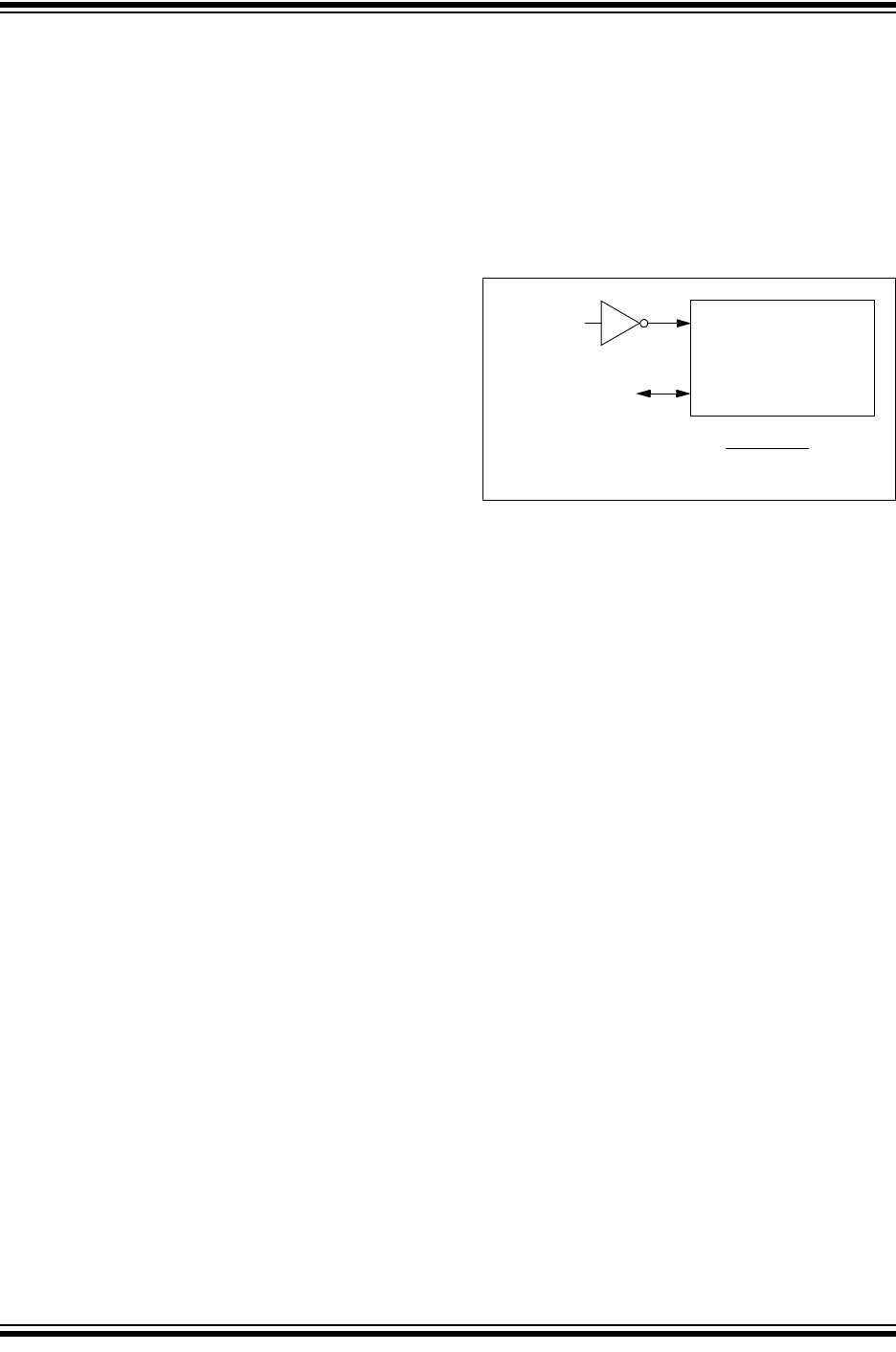
5.2.1.1 EC Mode
The External Clock (EC) mode allows an externally
generated logic level signal to be the system clock
source. When operating in this mode, an external clock
source is connected to the OSC1 input.
OSC2/CLKOUT is available for general purpose I/O or
CLKOUT. Figure 5-2 shows the pin connections for EC
mode.
EC mode has three power modes to select from through
Configuration Words:
• High power, 4-20 MHz (FOSC = 111)
• Medium power, 0.5-4 MHz (FOSC = 110)
• Low power, 0-0.5 MHz (FOSC = 101)
The Oscillator Start-up Timer (OST) is disabled when
EC mode is selected. Therefore, there is no delay in
operation after a Power-on Reset (POR) or wake-up
from Sleep. Because the PIC
®
MCU design is fully
static, stopping the external clock input will have the
effect of halting the device while leaving all data intact.
Upon restarting the external clock, the device will
resume operation as if no time had elapsed.
FIGURE 5-2: EXTERNAL CLOCK (EC)
MODE OPERATION
5.2.1.2 LP, XT, HS Modes
The LP, XT and HS modes support the use of quartz
crystal resonators or ceramic resonators connected to
OSC1 and OSC2 (Figure 5-3). The three modes select
a low, medium or high gain setting of the internal
inverter-amplifier to support various resonator types
and speed.
LP Oscillator mode selects the lowest gain setting of the
internal inverter-amplifier. LP mode current consumption
is the least of the three modes. This mode is designed to
drive only 32.768 kHz tuning-fork type crystals (watch
crystals).
XT Oscillator mode selects the intermediate gain
setting of the internal inverter-amplifier. XT mode
current consumption is the medium of the three modes.
This mode is best suited to drive resonators with a
medium drive level specification.
HS Oscillator mode selects the highest gain setting of the
internal inverter-amplifier. HS mode current consumption
is the highest of the three modes. This mode is best
suited for resonators that require a high drive setting.
Figure 5-3 and Figure 5-4 show typical circuits for
quartz crystal and ceramic resonators, respectively.
OSC1/CLKIN
OSC2/CLKOUT
Clock from
Ext. System
PIC
®
MCU
FOSC/4 or
I/O
(1)
Note 1: Output depends upon CLKOUTEN bit of the
Configuration Words.