
Datasheet


Table Of Contents
- High-Performance RISC CPU:
- Flexible Oscillator Structure:
- Special Microcontroller Features:
- Extreme Low-Power Management PIC16LF1526/7 with XLP:
- Analog Features:
- Peripheral Features:
- PIC16(L)F151X/152X Family Types
- Table of Contents
- Most Current Data Sheet
- Errata
- Customer Notification System
- 1.0 Device Overview
- 2.0 Enhanced Mid-Range CPU
- 3.0 Memory Organization
- 4.0 Device Configuration
- 5.0 Oscillator Module (with Fail-Safe Clock Monitor)
- 6.0 Resets
- FIGURE 6-1: Simplified Block Diagram of On-Chip Reset Circuit
- 6.1 Power-On Reset (POR)
- 6.2 Brown-Out Reset (BOR)
- 6.3 Register Definitions: BOR Control
- 6.4 Low-Power Brown-Out Reset (LPBOR)
- 6.5 MCLR
- 6.6 Watchdog Timer (WDT) Reset
- 6.7 RESET Instruction
- 6.8 Stack Overflow/Underflow Reset
- 6.9 Programming Mode Exit
- 6.10 Power-up Timer
- 6.11 Start-up Sequence
- 6.12 Determining the Cause of a Reset
- 6.13 Power Control (PCON) Register
- 6.14 Register Definitions: Power Control
- 7.0 Interrupts
- FIGURE 7-1: Interrupt Logic
- 7.1 Operation
- 7.2 Interrupt Latency
- 7.3 Interrupts During Sleep
- 7.4 INT Pin
- 7.5 Automatic Context Saving
- 7.6 Register Definitions: Interrupt Control
- Register 7-1: INTCON: Interrupt Control Register
- Register 7-2: PIE1: Peripheral Interrupt Enable Register 1
- Register 7-3: PIE2: Peripheral Interrupt Enable Register 2
- Register 7-4: PIE3: Peripheral Interrupt Enable Register 3
- Register 7-5: PIE4: Peripheral Interrupt Enable Register 4
- Register 7-6: PIR1: Peripheral Interrupt Request Register 1
- Register 7-7: PIR2: Peripheral Interrupt Request Register 2
- Register 7-8: PIR3: Peripheral Interrupt Request Register 3
- Register 7-9: PIR4: Peripheral Interrupt Request Register 4
- TABLE 7-1: Summary of Registers Associated with Interrupts
- 8.0 Power-Down Mode (Sleep)
- 9.0 Low Dropout (LDO) Voltage Regulator
- 10.0 Watchdog Timer (WDT)
- 11.0 Flash Program Memory Control
- 11.1 PMADRL and PMADRH Registers
- 11.2 Flash Program Memory Overview
- 11.3 Modifying Flash Program Memory
- 11.4 User ID, Device ID and Configuration Word Access
- 11.5 Write Verify
- 11.6 Register Definitions: Flash Program Memory Control
- Register 11-1: PMDATL: Program Memory Data Low Byte Register
- Register 11-2: PMDATH: Program Memory Data High Byte Register
- Register 11-3: PMADRL: Program Memory Address Low Byte Register
- Register 11-4: PMADRH: Program Memory Address High Byte Register
- Register 11-5: PMCON1: Program Memory Control 1 Register
- Register 11-6: PMCON2: Program Memory Control 2 Register
- TABLE 11-3: Summary of Registers Associated with Flash Program Memory
- TABLE 11-4: Summary of Configuration Word with Flash Program Memory
- 12.0 I/O Ports
- TABLE 12-1: Port Availability per Device
- FIGURE 12-1: Generic I/O Port Operation
- 12.1 Alternate Pin Function
- 12.2 Register Definitions: Alternate Pin Function Control
- 12.3 PORTA Registers
- 12.4 Register Definitions: PORTA
- 12.5 PORTB Registers
- 12.6 Register Definitions: PORTB
- 12.7 PORTC Registers
- 12.8 Register Definitions: PORTC
- 12.9 PORTD Registers
- 12.10 Register Definitions: PORTD
- 12.11 PORTE Registers
- 12.12 Register Definitions: PORTE
- 12.13 PORTF Registers
- 12.14 Register Definitions: PORTF
- 12.15 PORTG Registers
- 12.16 Register Definitions: PORTG
- Register 12-28: PORTG: PORTG Register
- Register 12-29: TRISG: PORTG Tri-State Register
- Register 12-30: LATG: PORTG Data Latch Register
- Register 12-31: ANSELG: PORTG Analog Select Register
- Register 12-32: WPUG: Weak Pull-up PORTG Register
- TABLE 12-17: Summary of Registers Associated with PORTG
- TABLE 12-18: Summary of cONFIGURATION wORD with PORTG
- 13.0 Interrupt-On-Change
- 14.0 Fixed Voltage Reference (FVR)
- 15.0 Temperature Indicator Module
- 16.0 Analog-to-Digital Converter (ADC) Module
- FIGURE 16-1: ADC Block Diagram
- 16.1 ADC Configuration
- 16.2 ADC Operation
- 16.3 Register Definitions: ADC Control
- Register 16-1: ADCON0: ADC Control Register 0
- Register 16-2: ADCON1: ADC Control Register 1
- Register 16-3: ADRESH: ADC Result Register High (ADRESH) ADFM = 0
- Register 16-4: ADRESL: ADC Result Register Low (ADRESL) ADFM = 0
- Register 16-5: ADRESH: ADC Result Register High (ADRESH) ADFM = 1
- Register 16-6: ADRESL: ADC Result Register Low (ADRESL) ADFM = 1
- 16.4 ADC Acquisition Requirements
- 17.0 Timer0 Module
- 18.0 Timer1/3/5 Module with Gate Control
- FIGURE 18-1: Timer1/3/5 Block Diagram
- FIGURE 18-2: Timer1/3/5 Clock Source Diagram
- 18.1 Timer1/3/5 Operation
- 18.2 Clock Source Selection
- 18.3 Timer1/3/5 Prescaler
- 18.4 Timer1/3/5 Oscillator
- 18.5 Timer1/3/5 Operation in Asynchronous Counter Mode
- 18.6 Timer1/3/5 Gate
- 18.7 Timer1/3/5 Interrupt
- 18.8 Timer1/3/5 Operation During Sleep
- 18.9 ECCP/CCP Capture/Compare Time Base
- 18.10 ECCP/CCP Special Event Trigger
- 18.11 Register Definitions: Timer1/3/5 Control
- 18.12 Register Definitions: Timer1/3/5 Gate Control
- 19.0 Timer2/4/6/8/10 Modules
- 20.0 Capture/Compare/PWM Modules
- 20.1 Capture Mode
- 20.2 Compare Mode
- 20.3 PWM Overview
- 20.4 Register Definitions: ECCP Control
- 21.0 Master Synchronous Serial Port (MSSP1 and MSSP2) Module
- 21.1 Master SSPx (MSSPx) Module Overview
- 21.2 SPI Mode Overview
- 21.3 I2C Mode Overview
- 21.4 I2C Mode Operation
- 21.5 I2C Slave Mode Operation
- 21.5.1 Slave Mode Addresses
- 21.5.2 Slave Reception
- FIGURE 21-14: I2C Slave, 7-bit Address, Reception (SEN = 0, AHEN = 0, DHEN = 0)
- FIGURE 21-15: I2C Slave, 7-bit Address, Reception (SEN = 1, AHEN = 0, DHEN = 0)
- FIGURE 21-16: I2C Slave, 7-bit Address, Reception (SEN = 0, AHEN = 1, DHEN = 1)
- FIGURE 21-17: I2C Slave, 7-bit Address, Reception (SEN = 1, AHEN = 1, DHEN = 1)
- 21.5.3 Slave Transmission
- 21.5.4 Slave Mode 10-bit Address Reception
- 21.5.5 10-bit Addressing with Address or Data Hold
- 21.5.6 Clock Stretching
- 21.5.7 Clock Synchronization and the CKP bit
- 21.5.8 General Call Address Support
- 21.5.9 SSPx Mask Register
- 21.6 I2C Master Mode
- 21.6.1 I2C Master Mode Operation
- 21.6.2 Clock Arbitration
- 21.6.3 WCOL Status Flag
- 21.6.4 I2C Master Mode Start Condition Timing
- 21.6.5 I2C Master Mode Repeated Start Condition Timing
- 21.6.6 I2C Master Mode Transmission
- 21.6.7 I2C Master Mode Reception
- 21.6.8 Acknowledge Sequence Timing
- 21.6.9 Stop Condition Timing
- 21.6.10 Sleep Operation
- 21.6.11 Effects of a Reset
- 21.6.12 Multi-Master Mode
- 21.6.13 Multi -Master Communication, Bus Collision and Bus Arbitration
- FIGURE 21-32: Bus Collision Timing for Transmit and Acknowledge
- FIGURE 21-33: Bus Collision During Start Condition (SDAx Only)
- FIGURE 21-34: Bus Collision During Start Condition (SCLx = 0)
- FIGURE 21-35: BRG Reset Due to Sda Arbitration During Start Condition
- FIGURE 21-36: Bus Collision During a Repeated Start Condition (Case 1)
- FIGURE 21-37: Bus Collision During Repeated Start Condition (Case 2)
- FIGURE 21-38: Bus Collision During a Stop Condition (Case 1)
- FIGURE 21-39: Bus Collision During a Stop Condition (Case 2)
- TABLE 21-3: Summary of Registers Associated with I2C™ Operation
- 21.7 Baud Rate Generator
- 21.8 Register Definitions: MSSP Control
- Register 21-1: SSPxSTAT: SSPx Status Register
- Register 21-2: SSPxCON1: SSPx Control Register 1
- Register 21-3: SSPxCON2: SSPx Control Register 2
- Register 21-4: SSPxCON3: SSPx Control Register 3
- Register 21-5: SSPxMSK: SSPx Mask Register
- Register 21-6: SSPxADD: MSSPx Address and Baud Rate Register (I2C Mode)
- 22.0 Enhanced Universal Synchronous Asynchronous Receiver Transmitter (EUSART)
- FIGURE 22-1: EUSART Transmit Block Diagram
- FIGURE 22-2: EUSART Receive Block Diagram
- 22.1 EUSART Asynchronous Mode
- 22.2 Clock Accuracy with Asynchronous Operation
- 22.3 Register Definitions: EUSART Control
- 22.4 EUSART Baud Rate Generator (BRG)
- EXAMPLE 22-1: Calculating Baud Rate Error
- TABLE 22-3: Baud Rate Formulas
- TABLE 22-4: Summary of Registers Associated with the Baud Rate Generator
- TABLE 22-5: Baud Rates for Asynchronous Modes
- 22.4.1 Auto-Baud Detect
- 22.4.2 Auto-Baud Overflow
- 22.4.3 Auto-Wake-up on Break
- 22.4.4 Break Character Sequence
- 22.4.5 Receiving a Break Character
- 22.5 EUSART Synchronous Mode
- 22.5.1 Synchronous Master Mode
- FIGURE 22-10: Synchronous Transmission
- FIGURE 22-11: Synchronous Transmission (through TXEN)
- TABLE 22-7: Summary of Registers Associated with Synchronous Master Transmission
- FIGURE 22-12: Synchronous Reception (Master Mode, SREN)
- TABLE 22-8: Summary of Registers Associated with Synchronous Master Reception
- 22.5.2 Synchronous Slave Mode
- 22.5.1 Synchronous Master Mode
- 23.0 In-Circuit Serial Programming™ (ICSP™)
- 24.0 Instruction Set Summary
- 25.0 Electrical Specifications
- Absolute Maximum Ratings(†)
- 25.1 DC Characteristics: Supply Voltage
- 25.2 DC Characteristics: Supply Current (Idd)
- 25.3 DC Characteristics: Power-Down Currents (Ipd)
- 25.4 DC Characteristics: I/O Ports
- 25.5 Memory Programming Requirements
- 25.6 Thermal Considerations
- 25.7 Timing Parameter Symbology
- 25.8 AC Characteristics: PIC16(L)F1526/7-I/E
- FIGURE 25-6: Clock Timing
- TABLE 25-1: Clock Oscillator Timing Requirements
- TABLE 25-2: Oscillator Parameters
- FIGURE 25-7: CLKOUT and I/O Timing
- TABLE 25-3: CLKOUT and I/O Timing Parameters
- FIGURE 25-8: Reset, Watchdog Timer, Oscillator Start-up Timer and Power-up Timer Timing
- FIGURE 25-9: Brown-Out Reset Timing and Characteristics
- TABLE 25-4: Reset, Watchdog Timer, Oscillator Start-up Timer, Power-up Timer and Brown-Out Reset Parameters
- FIGURE 25-10: Timer0 and Timer1 External Clock Timings
- TABLE 25-5: Timer0 and Timer1 External Clock Requirements
- FIGURE 25-11: Capture/Compare/PWM Timings (CCP)
- TABLE 25-6: Capture/Compare/PWM Requirements (CCP)
- TABLE 25-7: Analog-to-Digital Converter (ADC) Characteristics(1,2,3)
- TABLE 25-8: ADC Conversion Requirements
- FIGURE 25-12: ADC Conversion Timing (Normal Mode)
- FIGURE 25-13: ADC Conversion Timing (Sleep Mode)
- TABLE 25-9: Low Dropout (LDO) Regulator Characteristics
- FIGURE 25-14: USART Synchronous Transmission (Master/Slave) Timing
- TABLE 25-10: USART Synchronous Transmission Requirements
- FIGURE 25-15: USART Synchronous Receive (Master/Slave) Timing
- TABLE 25-11: USART Synchronous Receive Requirements
- FIGURE 25-16: SPI Master Mode Timing (CKE = 0, SMP = 0)
- FIGURE 25-17: SPI Master Mode Timing (CKE = 1, SMP = 1)
- FIGURE 25-18: SPI Slave Mode Timing (CKE = 0)
- FIGURE 25-19: SPI Slave Mode Timing (CKE = 1)
- TABLE 25-12: SPI Mode requirements
- FIGURE 25-20: I2C™ Bus Start/Stop Bits Timing
- TABLE 25-13: I2C™ Bus Start/Stop Bits Requirements
- FIGURE 25-21: I2C™ Bus Data Timing
- TABLE 25-14: I2C™ Bus Data Requirements
- 26.0 DC and AC Characteristics Graphs and Charts
- FIGURE 26-1: Idd, LP Oscillator, Fosc = 32 kHz, PIC16LF1526 ONLY
- FIGURE 26-2: Idd, LP Oscillator, Fosc = 32 kHz, PIC16F1526/7 ONLY
- FIGURE 26-3: Idd Typical, XT and EXTRC Oscillator, PIC16LF1526 ONLY
- FIGURE 26-4: Idd Maximum, XT and EXTRC Oscillator, PIC16LF1526 ONLY
- FIGURE 26-5: Idd Typical, XT and EXTRC Oscillator, PIC16F1526/7 ONLY
- FIGURE 26-6: Idd Maximum, XT and EXTRC Oscillator, PIC16F1526/7 ONLY
- FIGURE 26-7: Idd, External Clock (ECL), Low-Power Mode, Fosc = 32 kHz, PIC16LF1526 ONLY
- FIGURE 26-8: Idd, External Clock (ECL), Low-Power Mode, Fosc = 32 kHz, PIC16F1526/7 ONLY
- FIGURE 26-9: Idd, External Clock (ECL), Low-Power Mode, Fosc = 500 kHz, PIC16LF1526 ONLY
- FIGURE 26-10: Idd, External Clock (ECL), Low-Power Mode, Fosc = 500 kHz, PIC16F1526/7 ONLY
- FIGURE 26-11: Idd Typical, External Clock (ECM), Medium-Power Mode, PIC16LF1526 ONLY
- FIGURE 26-12: Idd Maximum, External Clock (ECM), Medium-Power Mode, PIC16LF1526 ONLY
- FIGURE 26-13: Idd Typical, External Clock (ECM), Medium-Power Mode, PIC16F1526/7 ONLY
- FIGURE 26-14: Idd Maximum, External Clock (ECM), Medium-Power Mode, PIC16F1526/7 ONLY
- FIGURE 26-15: Idd Typical, External Clock (ECH), High-Power Mode, PIC16LF1526 ONLY
- FIGURE 26-16: Idd Maximum, External Clock (ECH), High-Power Mode, PIC16LF1526 ONLY
- FIGURE 26-17: Idd Typical, External Clock (ECH), High-Power Mode, PIC16F1526/7 ONLY
- FIGURE 26-18: Idd Maximum, External Clock (ECH), High-Power Mode, PIC16F1526/7 ONLY
- FIGURE 26-19: Idd, LFINTOSC, Fosc = 31 kHz, PIC16LF1526 Only
- FIGURE 26-20: Idd, LFINTOSC, Fosc = 31 kHz, PIC16F1526/7 Only
- FIGURE 26-21: Idd, MFINTOSC, Fosc = 500 kHz, PIC16LF1526 ONLY
- FIGURE 26-22: Idd, MFINTOSC, Fosc = 500 kHz, PIC16F1526/7 ONLY
- FIGURE 26-23: Idd Typical, HFINTOSC, PIC16LF1526 ONLY
- FIGURE 26-24: Idd Maximum, HFINTOSC, PIC16LF1526 ONLY
- FIGURE 26-25: Idd Typical, HFINTOSC, PIC16F1526/7 ONLY
- FIGURE 26-26: Idd Maximum, HFINTOSC, PIC16F1526/7 ONLY
- FIGURE 26-27: Idd Typical, HS OScillator, PIC16LF1526 ONLY
- FIGURE 26-28: Idd Maximum, HS Oscillator, PIC16LF1526 ONLY
- FIGURE 26-29: Idd Typical, HS Oscillator, PIC16F1526/7 ONLY
- FIGURE 26-30: Idd Maximum, HS Oscillator, PIC16F1526/7 ONLY
- FIGURE 26-31: Ipd Base, Sleep Mode, PIC16LF1526 ONly
- FIGURE 26-32: Ipd Base, Low-Power Sleep Mode, VREGPM = 1, PIC16F1526/7 ONLy
- FIGURE 26-33: Ipd, Watchdog Timer (WDT), PIC16LF1526 ONLy
- FIGURE 26-34: Ipd, Watchdog Timer (WDT), PIC16F1526/7 ONLy
- FIGURE 26-35: Ipd, Fixed Voltage Reference (FVR), PIC16LF1526 ONLy
- FIGURE 26-36: Ipd, Fixed Voltage Reference (FVR), PIC16F1526/7 ONLy
- FIGURE 26-37: Ipd, Brown-Out Reset (BOR), BORV = 1, PIC16LF1526 ONLY
- FIGURE 26-38: Ipd, Brown-Out Reset (BOR), BORV = 1, PIC16F1526/7 ONLy
- FIGURE 26-39: Ipd, Secondary Oscillator, Fosc = 32 kHz, PIC16LF1526 ONLy
- FIGURE 26-40: Ipd, Secondary Oscillator, Fosc = 32 kHz, PIC16F1526/7 ONly
- FIGURE 26-41: Voh vs. Ioh over Temperature, Vdd = 5.5V, PIC16F1526/7 ONLy
- FIGURE 26-42: Vol vs. Iol over Temperature, Vdd = 5.5V, PIC16F1526/7 ONLy
- FIGURE 26-43: Voh vs. Ioh over Temperature, Vdd = 3.0V
- FIGURE 26-44: Vol vs. Iol over Temperature, Vdd = 3.0V
- FIGURE 26-45: Voh vs. Ioh over Temperature, Vdd = 1.8V, PIC16LF1526 Only
- FIGURE 26-46: Vol vs. Iol over Temperature, Vdd = 1.8V, PIC16LF1526 Only
- FIGURE 26-47: POR Release Voltage
- FIGURE 26-48: POR Rearm Voltage, PIC16F1526/7 ONLy
- FIGURE 26-49: Brown-Out Reset Voltage, BORV = 1, PIC16LF1526 Only
- FIGURE 26-50: Brown-Out Reset Hysteresis, BORV = 1, PIC16LF1526 Only
- FIGURE 26-51: Brown-Out Reset Voltage, BORV = 1, PIC16F1526/7 Only
- FIGURE 26-52: Brown-Out Reset Hysteresis, BORV = 1, PIC16F1526/7 Only
- FIGURE 26-53: Brown-Out Reset Voltage, BORV = 0
- FIGURE 26-54: Brown-Out Reset Hysteresis, BORV = 0
- FIGURE 26-55: Low-Power Brown-Out Reset Voltage, LPBOR = 0
- FIGURE 26-56: Low-Power Brown-Out Reset Hysteresis, LPBOR = 0
- FIGURE 26-57: WDT Time-Out Period
- FIGURE 26-58: PWRT Period
- FIGURE 26-59: FVR Stabilization Period
- FIGURE 26-60: LFINTOSC Frequency Over Vdd and Temperature, PIC16LF1526 Only
- FIGURE 26-61: LFINTOSC Frequency Over Vdd and Temperature, PIC16F1526/7 Only
- FIGURE 26-62: Sleep Mode, Wake Period with HFINTOSC Source, PIC16LF1526/7 Only
- FIGURE 26-63: Low-Power Sleep Mode, Wake Period with HFINTOSC Source, VREGPM = 1, PIC16F1526/7 Only
- FIGURE 26-64: Sleep Mode, Wake Period with HFINTOSC Source, VREGPM = 0, PIC16F1526/7 Only
- 27.0 Development Support
- 27.1 MPLAB Integrated Development Environment Software
- 27.2 MPLAB C Compilers for Various Device Families
- 27.3 HI-TECH C for Various Device Families
- 27.4 MPASM Assembler
- 27.5 MPLINK Object Linker/ MPLIB Object Librarian
- 27.6 MPLAB Assembler, Linker and Librarian for Various Device Families
- 27.7 MPLAB SIM Software Simulator
- 27.8 MPLAB REAL ICE In-Circuit Emulator System
- 27.9 MPLAB ICD 3 In-Circuit Debugger System
- 27.10 PICkit 3 In-Circuit Debugger/ Programmer and PICkit 3 Debug Express
- 27.11 PICkit 2 Development Programmer/Debugger and PICkit 2 Debug Express
- 27.12 MPLAB PM3 Device Programmer
- 27.13 Demonstration/Development Boards, Evaluation Kits, and Starter Kits
- 28.0 Packaging Information
- Appendix A: Data Sheet Revision History
- INDEX
- The Microchip Web Site
- Customer Change Notification Service
- Customer Support
- Reader Response
- Product Identification System
- Trademarks
- Worldwide Sales
PIC16(L)F1526/7
DS41458C-page 30 2011-2013 Microchip Technology Inc.
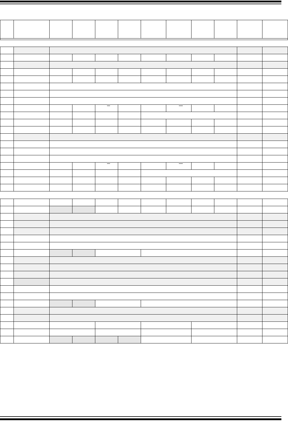
Bank 4
20Ch — Unimplemented — —
20Dh WPUB WPUB7 WPUB6 WPUB5 WPUB4 WPUB3 WPUB2 WPUB1 WPUB0 1111 1111 1111 1111
20Eh
— Unimplemented — —
20Fh WPUD WPUD7 WPUD6 WPUD5 WPUD4 WPUD3 WPUD2 WPUD1 WPUD0 1111 1111 1111 1111
210h WPUE WPUE7 WPUE6 WPUE5 WPUE4 WPUE3 WPUE2 WPUE1 WPUE0 1111 1111 1111 1111
211h SSP1BUF Synchronous Serial Port Receive Buffer/Transmit Register xxxx xxxx uuuu uuuu
212h SSP1ADD Synchronous Serial Port (I
2
C mode) Address Register 0000 0000 0000 0000
213h SSP1MSK Synchronous Serial Port (I
2
C mode) Address Mask Register 1111 1111 1111 1111
214h SSP1STAT SMP CKE D/A
PSR/WUA BF 0000 0000 0000 0000
215h SSP1CON1 WCOL SSPOV SSPEN CKP SSPM<3:0> 0000 0000 0000 0000
216h SSP1CON2 GCEN ACKSTAT ACKDT ACKEN RCEN PEN RSEN SEN 0000 0000 0000 0000
217h SSP1CON3 ACKTIM PCIE SCIE BOEN SDAHT SBCDE AHEN DHEN 0000 0000 0000 0000
218h
— Unimplemented — —
219h SSP2BUF Synchronous Serial Port Receive Buffer/Transmit Register xxxx xxxx uuuu uuuu
21Ah SSP2ADD Synchronous Serial Port (I
2
C mode) Address Register 0000 0000 0000 0000
21Bh SSP2MSK Synchronous Serial Port (I
2
C mode) Address Mask Register 1111 1111 1111 1111
21Ch SSP2STAT SMP CKE D/A
PSR/WUA BF 0000 0000 0000 0000
21Dh SSP2CON1 WCOL SSPOV SSPEN CKP SSPM<3:0> 0000 0000 0000 0000
21Eh SSP2CON2 GCEN ACKSTAT ACKDT ACKEN RCEN PEN RSEN SEN 0000 0000 0000 0000
21Fh SSP2CON3 ACKTIM PCIE SCIE BOEN SDAHT SBCDE AHEN DHEN 0000 0000 0000 0000
Bank 5
28Ch PORTF RF7 RF6 RF5 RF4 RF3 RF2 RF1 RF0 xxxx xxxx uuuu uuuu
28Dh PORTG
— — RG5 RG4 RG3 RG2 RG1 RG0 --xx xxxx --uu uuuu
28Eh
— Unimplemented — —
28Fh
— Unimplemented — —
290h
— Unimplemented — —
291h CCPR1L Capture/Compare/PWM Register 1 (LSB) xxxx xxxx uuuu uuuu
292h CCPR1H Capture/Compare/PWM Register 1 (MSB) xxxx xxxx uuuu uuuu
293h CCP1CON
— — DC1B<1:0> CCP1M<3:0> --00 0000 --00 0000
294h
— Unimplemented — —
295h
— Unimplemented — —
296h
— Unimplemented — —
297h
— Unimplemented — —
298h CCPR2L Capture/Compare/PWM Register 2 (LSB) xxxx xxxx uuuu uuuu
299h CCPR2H Capture/Compare/PWM Register 2 (MSB) xxxx xxxx uuuu uuuu
29Ah CCP2CON
— — DC2B<1:0> CCP2M<3:0> --00 0000 --00 0000
29Bh
— Unimplemented — —
29Ch
— Unimplemented — —
29Dh CCPTMRS0 C4TSEL<1:0> C3TSEL<1:0> C2TSEL<1:0> C1TSEL<1:0> 0000 0000 0000 0000
29Eh CCPTMRS1 C8TSEL<1:0> C7TSEL<1:0> C6TSEL<1:0> C5TSEL<1:0> 0000 0000 0000 0000
29Fh CCPTMRS2
— — — — C10TSEL<1:0> C9TSEL<1:0> ---- 0000 ---- 0000
TABLE 3-2: SPECIAL FUNCTION REGISTER SUMMARY (CONTINUED)
Addr Name Bit 7 Bit 6 Bit 5 Bit 4 Bit 3 Bit 2 Bit 1 Bit 0
Value on
POR, BOR
Value on
all other
Resets
Legend: x = unknown, u = unchanged, q = value depends on condition, - = unimplemented, read as ‘0’, r = reserved.
Shaded locations are unimplemented, read as ‘0’.
Note 1: PIC16F1526/7 only.
2: Unimplemented, read as ‘1’.