
Datasheet


2010-2012 Microchip Technology Inc. DS41452C-page 161
PIC16(L)F1516/7/8/9
18.11 Register Definitions: Timer1 Control
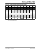
REGISTER 18-1: T1CON: TIMER1 CONTROL REGISTER
R/W-0/u R/W-0/u R/W-0/u R/W-0/u R/W-0/u R/W-0/u U-0 R/W-0/u
TMR1CS<1:0> T1CKPS<1:0> T1OSCEN T1SYNC
—TMR1ON
bit 7 bit 0
Legend:
R = Readable bit W = Writable bit U = Unimplemented bit, read as ‘0’
u = Bit is unchanged x = Bit is unknown -n/n = Value at POR and BOR/Value at all other Resets
‘1’ = Bit is set ‘0’ = Bit is cleared
bit 7-6
TMR1CS<1:0>: Timer1 Clock Source Select bits
11 = Timer1 clock source is LFINTOSC
10 = Timer1 clock source is pin or oscillator:
If T1OSCEN =
0:
External clock from T1CKI pin (on the rising edge)
If T1OSCEN =
1:
Crystal oscillator on SOSCI/SOSCO pins
01 = Timer1 clock source is system clock (F
OSC)
00 = Timer1 clock source is instruction clock (F
OSC/4)
bit 5-4
T1CKPS<1:0>: Timer1 Input Clock Prescale Select bits
11 = 1:8 Prescale value
10 = 1:4 Prescale value
01 = 1:2 Prescale value
00 = 1:1 Prescale value
bit 3
T1OSCEN: LP Oscillator Enable Control bit
1 = Secondary oscillator circuit enabled for Timer1
0 = Secondary oscillator circuit disabled for Timer1
bit 2
T1SYNC: Timer1 External Clock Input Synchronization Control bit
TMR1CS<1:0> =
1X:
1 = Do not synchronize external clock input
0 = Synchronize external clock input with system clock (F
OSC)
TMR1CS<1:0> =
0X:
This bit is ignored. Timer1 uses the internal clock when TMR1CS<1:0> = 1X.
bit 1
Unimplemented: Read as ‘0’
bit 0
TMR1ON: Timer1 On bit
1 = Enables Timer1
0 = Stops Timer1
Clears Timer1 gate flip-flop