
Datasheet


PIC16(L)F1516/7/8/9
DS41452C-page 146 2010-2012 Microchip Technology Inc.
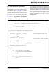
FIGURE 16-4: ANALOG INPUT MODEL
FIGURE 16-5: ADC TRANSFER FUNCTION
Note 1: The reference voltage (VREF) has no effect on the equation, since it cancels itself out.
2: The charge holding capacitor (CHOLD) is not discharged after each conversion.
3: The maximum recommended impedance for analog sources is 10 k. This is required to meet the pin
leakage specification.
CPIN
VA
Rs
Analog
5 pF
V
DD
VT 0.6V
V
T 0.6V
I
LEAKAGE
(1)
RIC 1k
Sampling
Switch
SS
Rss
C
HOLD = 10 pF
V
SS/VREF-
6V
Sampling Switch
5V
4V
3V
2V
567891011
(k
)
V
DD
Legend:
CPIN
VT
I LEAKAGE
RIC
SS
C
HOLD
= Input Capacitance
= Threshold Voltage
= Leakage current at the pin due to
= Interconnect Resistance
= Sampling Switch
= Sample/Hold Capacitance
various junctions
RSS
Note 1: Refer to Section 25.0 “Electrical Specifications”.
RSS = Resistance of Sampling Switch
Input
pin
3FFh
3FEh
ADC Output Code
3FDh
3FCh
03h
02h
01h
00h
Full-Scale
3FBh
0.5 LSB
V
REF-
Zero-Scale
Transition
V
REF+
Transition
1.5 LSB
Full-Scale Range
Analog Input Voltage