
Datasheet


PIC16(L)F1516/7/8/9
DS41452C-page 132 2010-2012 Microchip Technology Inc.
14.3 Register Definitions: FVR Control
TABLE 14-2: SUMMARY OF REGISTERS ASSOCIATED WITH FIXED VOLTAGE REFERENCE
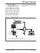
REGISTER 14-1: FVRCON: FIXED VOLTAGE REFERENCE CONTROL REGISTER
R/W-0/0 R-q/q R/W-0/0 R/W-0/0 U-0 U-0 R/W-0/0 R/W-0/0
FVREN FVRRDY
(1)
TSEN TSRNG — —ADFVR<1:0>
bit 7 bit 0
Legend:
R = Readable bit W = Writable bit U = Unimplemented bit, read as ‘0’
u = Bit is unchanged x = Bit is unknown -n/n = Value at POR and BOR/Value at all other Resets
‘1’ = Bit is set ‘0’ = Bit is cleared q = Value depends on condition
bit 7
FVREN: Fixed Voltage Reference Enable bit
0 = Fixed Voltage Reference is disabled
1 = Fixed Voltage Reference is enabled
bit 6
FVRRDY: Fixed Voltage Reference Ready Flag bit
(1)
0 = Fixed Voltage Reference output is not ready or not enabled
1 = Fixed Voltage Reference output is ready for use
bit 5
TSEN: Temperature Indicator Enable bit
0 = Temperature Indicator is disabled
1 = Temperature Indicator is enabled
bit 4
TSRNG: Temperature Indicator Range Selection bit
0 =V
OUT = VDD - 2VT (Low Range)
1 =V
OUT = VDD - 4VT (High Range)
bit 3-2
Unimplemented: Read as ‘0’
bit 1-0
ADFVR<1:0>: ADC Fixed Voltage Reference Selection bits
00 = ADC Fixed Voltage Reference Peripheral output is off
01 = ADC Fixed Voltage Reference Peripheral output is 1x (1.024V)
10 = ADC Fixed Voltage Reference Peripheral output is 2x (2.048V)
(2)
11 = ADC Fixed Voltage Reference Peripheral output is 4x (4.096V)
(2)
Note 1: FVRRDY is always ‘1’ on PIC16F1516/7/8/9 only.
2: Fixed Voltage Reference output cannot exceed VDD.
Name Bit 7 Bit 6 Bit 5 Bit 4 Bit 3 Bit 2 Bit 1 Bit 0
Register
on page
FVRCON FVREN FVRRDY TSEN TSRNG — —ADFVR<1:0>132
Legend: Shaded cells are unused by the Fixed Voltage Reference module.