
Datasheet


2010-2012 Microchip Technology Inc. DS41452C-page 123
PIC16(L)F1516/7/8/9
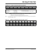
REGISTER 12-19: PORTE: PORTE REGISTER
U-0 U-0 U-0 U-0 R-x/u R/W-x/u R/W-x/u R/W-x/u
— — — —
RE3 RE2
(1)
RE1
(1)
RE0
(1)
bit 7 bit 0
Legend:
R = Readable bit W = Writable bit U = Unimplemented bit, read as ‘0’
u = Bit is unchanged x = Bit is unknown -n/n = Value at POR and BOR/Value at all other Resets
‘1’ = Bit is set ‘0’ = Bit is cleared
bit 7-4 Unimplemented: Read as ‘0’
bit 3-0 RE<3:0>: PORTE I/O Pin bits
(1)
1 = Port pin is > VIH
0 = Port pin is < VIL
Note 1: RE<2:0> are not implemented on the PIC16(L)F1516/8. Read as ‘0’. Writes to RE<2:0> are actually writ-
ten to corresponding LATE register. Reads from PORTE register is the return of actual I/O pin values.
REGISTER 12-20: TRISE: PORTE TRI-STATE REGISTER
U-0 U-0 U-0 U-0 U-1
(2)
R/W-1 R/W-1 R/W-1
— — — — —
TRISE2
(1)
TRISE1
(1)
TRISE0
(1)
bit 7 bit 0
Legend:
R = Readable bit W = Writable bit U = Unimplemented bit, read as ‘0’
u = bit is unchanged x = Bit is unknown -n/n = Value at POR and BOR/Value at all other Resets
‘1’ = Bit is set ‘0’ = Bit is cleared
bit 7-4 Unimplemented: Read as ‘0’
bit 3 Unimplemented: Read as ‘1’
bit 2-0 TRISE<2:0>: RE<2:0> Tri-State Control bits
(1)
1 = PORTE pin configured as an input (tri-stated)
0 = PORTE pin configured as an output
Note 1: TRISE<2:0> are not implemented on the PIC16(L)F1517/9. Read as ‘0’.
2: Unimplemented, read as ‘1’.