
Datasheet


2010-2012 Microchip Technology Inc. DS41452C-page 105
PIC16(L)F1516/7/8/9
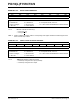
REGISTER 11-5: PMCON1: PROGRAM MEMORY CONTROL 1 REGISTER
U-1 R/W-0/0 R/W-0/0 R/W/HC-0/0 R/W/HC-x/q
(2)
R/W-0/0 R/S/HC-0/0 R/S/HC-0/0
—
(1)
CFGS LWLO FREE WRERR WREN WR RD
bit 7 bit 0
Legend:
R = Readable bit W = Writable bit U = Unimplemented bit, read as ‘0’
S = Bit can only be set x = Bit is unknown -n/n = Value at POR and BOR/Value at all other Resets
‘1’ = Bit is set ‘0’ = Bit is cleared HC = Bit is cleared by hardware
bit 7 Unimplemented: Read as ‘1’
bit 6
CFGS: Configuration Select bit
1 = Access Configuration, User ID and Device ID Registers
0 = Access Flash program memory
bit 5
LWLO: Load Write Latches Only bit
(3)
1 = Only the addressed program memory write latch is loaded/updated on the next WR command
0 = The addressed program memory write latch is loaded/updated and a write of all program memory write latches
will be initiated on the next WR command
bit 4
FREE: Program Flash Erase Enable bit
1 = Performs an erase operation on the next WR command (hardware cleared upon completion)
0 = Performs an write operation on the next WR command
bit 3
WRERR: Program/Erase Error Flag bit
1 = Condition indicates an improper program or erase sequence attempt or termination (bit is set automatically
on any set attempt (write ‘
1’) of the WR bit).
0 = The program or erase operation completed normally.
bit 2
WREN: Program/Erase Enable bit
1 = Allows program/erase cycles
0 = Inhibits programming/erasing of program Flash
bit 1
WR: Write Control bit
1 = Initiates a program Flash program/erase operation.
The operation is self-timed and the bit is cleared by hardware once operation is complete.
The WR bit can only be set (not cleared) in software.
0 = Program/erase operation to the Flash is complete and inactive.
bit 0
RD: Read Control bit
1 = Initiates a program Flash read. Read takes one cycle. RD is cleared in hardware. The RD bit can only be set
(not cleared) in software.
0 = Does not initiate a program Flash read.
Note 1: Unimplemented bit, read as ‘1’.
2: The WRERR bit is automatically set by hardware when a program memory write or erase operation is started (WR = 1) .
3: The LWLO bit is ignored during a program memory erase operation (FREE = 1).