
Datasheet


2012 Microchip Technology Inc. Preliminary DS41624B-page 275
PIC16(L)F1512/3
23.0 IN-CIRCUIT SERIAL
PROGRAMMING™ (ICSP™)
ICSP™ programming allows customers to manufacture
circuit boards with unprogrammed devices. Programming
can be done after the assembly process allowing the
device to be programmed with the most recent firmware
or a custom firmware. Five pins are needed for ICSP™
programming:
• ICSPCLK
• ICSPDAT
•MCLR
/VPP
•VDD
•VSS
In Program/Verify mode the program memory, user IDs
and the Configuration Words are programmed through
serial communications. The ICSPDAT pin is a
bidirectional I/O used for transferring the serial data and
the ICSPCLK pin is the clock input. For more information
on ICSP™ refer to the “
PIC16(L)F151X/152X Memory
Programming Specification
” (DS41442).
23.1 High-Voltage Programming Entry
Mode
The device is placed into High-Voltage Programming
Entry mode by holding the ICSPCLK and ICSPDAT
pins low then raising the voltage on MCLR
/VPP to VIHH.
23.2 Low-Voltage Programming Entry
Mode
The Low-Voltage Programming Entry mode allows the
PIC16(L)F151X devices to be programmed using V
DD
only, without high voltage. When the LVP bit of
Configuration Words is set to ‘1’, the low-voltage ICSP
programming entry is enabled. To disable the
Low-Voltage ICSP mode, the LVP bit must be
programmed to ‘0’.
Entry into the Low-Voltage Programming Entry mode
requires the following steps:
1. MCLR
is brought to VIL.
2. A 32-bit key sequence is presented on
ICSPDAT, while clocking ICSPCLK.
Once the key sequence is complete, MCLR
must be
held at V
IL for as long as Program/Verify mode is to be
maintained.
If low-voltage programming is enabled (LVP = 1), the
MCLR
Reset function is automatically enabled and
cannot be disabled. See
Section 6.3 “Low-Power
Brown-out Reset (LPBOR)”
for more information.
The LVP bit can only be reprogrammed to ‘0’ by using
the High-Voltage Programming mode.
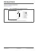
23.3 Common Programming Interfaces
Connection to a target device is typically done through
an ICSP™ header. A commonly found connector on
development tools is the RJ-11 in the 6P6C (6-pin, 6
connector) configuration. See Figure 23-1.
FIGURE 23-1: ICD RJ-11 STYLE
CONNECTOR INTERFACE
1
2
3
4
5
6
Target
Bottom Side
PC Board
VPP/MCLR
VSS
ICSPCLK
V
DD
ICSPDAT
NC
Pin Description*
1 = V
PP/MCLR
2 = VDD Target
3 = V
SS (ground)
4 = ICSPDAT
5 = ICSPCLK
6 = No Connect