
Datasheet


PIC16(L)F1512/3
DS41624B-page 144 Preliminary 2012 Microchip Technology Inc.
TABLE 16-5: ADC CLOCK PERIOD (TAD) VS. DEVICE OPERATING FREQUENCIES
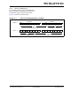
FIGURE 16-6: ANALOG-TO-DIGITAL SINGLE CONVERSION
(ADDSEN =
0
)
TAD CYCLES
ADC Clock Period (TAD) Device Frequency (FOSC)
ADC
Clock Source
ADCS<2:0> 20 MHz 16 MHz 8 MHz 4 MHz 1 MHz
Fosc/2 000 100 ns
(2)
125 ns
(2)
250 ns
(2)
500 ns
(2)
2.0 s
Fosc/4 100
200 ns
(2)
250 ns
(2)
500 ns
(2)
1.0 s4.0 s
Fosc/8 001
400 ns
(2)
0.5 s
(2)
1.0 s2.0 s 8.0 s
(3)
Fosc/16 101 800 ns 1.0 s2.0 s4.0 s 16.0 s
(3)
Fosc/32 010 1.6 s2.0 s4.0 s 8.0 s
(3)
32.0 s
(3)
Fosc/64 110 3.2 s4.0 s 8.0 s
(3)
16.0 s
(3)
64.0 s
(3)
FRC x11 1.0-6.0 s
(1,4)
1.0-6.0 s
(1,4)
1.0-6.0 s
(1,4)
1.0-6.0 s
(1,4)
1.0-6.0 s
(1,4)
Legend: Shaded cells are outside of recommended range.
Note 1: The FRC source has a typical TAD time of 1.6 s for VDD.
2: These values violate the minimum required TAD time.
3: For faster conversion times, the selection of another clock source is recommended.
4: The ADC clock period (TAD) and total ADC conversion time can be minimized when the ADC clock is
derived from the system clock F
OSC. However, the FRC clock source must be used when conversions are
to be performed with the device in Sleep mode.
T
AD
1
T
AD
2
T
AD
3 T
AD
4 T
AD
5
T
AD
6 T
AD
7
T
AD
8 T
AD
11
Set GO/DONE bit
Holding capacitor C
HOLD
is disconnected from analog input (typically 100 ns)
T
AD
9 T
AD
10
T
CY
- T
AD
AADRES0H:AADRES0L is loaded,
ADIF bit is set,
Conversion starts
b0
b9
b6
b5
b4
b3
b2
b1
b8
b7
On the following cycle:
1-127 T
INST
1-127 T
INST
Pre-Charge
Acquisition/
Sharing Time
Time
Conversion Time
If ADPRE =
0
If ADACQ =
0
If ADPRE =
0
If ADACQ =
0
GO/DONE bit is cleared
(Traditional Timing of ADC Conversion)
External and Internal
Channels are
charged/discharged
External and Internal
Channels share
charge
(Traditional Operation Start)
(T
PRE
)
(T
ACQ
)