
Datasheet


2012 Microchip Technology Inc. Preliminary DS41624B-page 143
PIC16(L)F1512/3
16.5 Capacitive Voltage Divider (CVD)
16.5.1 ADC REGISTER MAPPING
The ADC module with Capacitive Voltage Divider
(CVD) is an enhanced version of the standard ADC
module as stated in
Section 16.0 “Analog-to-Digital
Converter (ADC) Module”
through Section 16.3
“ADC Register Definitions”
and is backward
compatible with the other devices in this family. Control
of the standard ADC module uses Bank 1 registers,
see
Table 16-4. This set of registers are mapped into
Bank 14 with the control registers for the ADC module
with capacitive voltage divider control. Although this
subset of registers have different names, they are
identical. Since the registers for the standard ADC are
mapped into the Bank 14 address space, any changes
to registers in Bank 1 will be reflected in Bank 14 and
vice-versa.
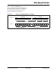
TABLE 16-4: ADC REGISTER MAPPING
16.5.2 CONVERSION CLOCK
The source of the conversion clock is software
selectable via the ADCS bits of the AADCON1 register.
There are seven possible clock options:
•F
OSC/2
•F
OSC/4
•F
OSC/8
•F
OSC/16
•F
OSC/32
•F
OSC/64
•F
RC (dedicated internal oscillator)
The time to complete one bit conversion is defined as
T
AD. One full 10-bit conversion requires 11.5 TAD
periods as shown in Figure 16-6.
For correct conversion, the appropriate T
AD specifica-
tion must be met. Refer to the A/D conversion require-
ments in
Section 25.0 “Electrical Specifications” for
more information. Table 16-5 gives examples of
appropriate ADC clock selections.
[Bank 14 Address] [Bank 1 Address]
ADC
with Capacitive Voltage
Divider
ADC
[711h] AADCON0
(1)
[09Dh] ADCON0
(1)
[712h] AADCON1
(1)
[09Eh] ADCON1
(1)
[713h] AADCON2
[714h] AADCON3
[715h] AADSTAT
[716h] AADPRE
[717h] AADACQ
[718h] AADGRD
[719h] AADCAP
[71Ah] AADRES0L
(1)
[09Bh] ADRES0L
(1)
[71Bh] AADRES0H
(1)
[09Ch] ADRES0H
(1)
[71Ch] AADRES1L
[71Dh] AADRES1L
Note 1: Register is mapped in Bank 1 and Bank
14, using different names in each bank.
Note: Unless using the FRC, any changes in the
system clock frequency will change the
ADC clock frequency, which may
adversely affect the ADC result.