
Information


2012 Microchip Technology Inc. DS80543B-page 3
PIC16(L)F1512/1513
Silicon Errata Issues
1. Module: Oscillator
1.1 Clock Switching
When switching clock sources between INTOSC
clock source and an external clock source, one
corrupted instruction may be executed after the
switch occurs.
Work around
When switching from an external oscillator clock
source, first switch to 16 MHz HFINTOSC. Once
running at 16 MHz HFINTOSC, configure IRCF to
run at desired internal oscillator frequency.
When switching from an internal oscillator
(INTOSC) to an external oscillator clock source,
first switch to HFINTOSC High-Power mode (16
MHz). Once running from HFINTOSC, switch to
the external oscillator clock source.
Affected Silicon Revisions
1.2 Oscillator Start-up Timer (OST) bit
During the Two-Speed Start-up sequence, the
OST is enabled to count 1024 clock cycles. After
the count is reached, the OSTS bit is set, the
system clock is held low until the next falling edge
of the external crystal (LP, XT or HS mode), before
switching to the external clock source.
When an external oscillator is configured as the
primary clock and Fail-Safe Clock mode is enabled
(FCMEN = 1), any of the following conditions will
result in the Oscillator Start-up Timer (OST) failing
to restart:
•MCLR
Reset
• Wake from Sleep
• Clock change from INTOSC to Primary Clock
This anomaly will manifest itself as a clock failure
condition for external oscillators which take longer
than the clock failure time-out period to start.
Work around
None.
Affected Silicon Revisions
2. Module: ADC
2.1 ADOEN Bit Issue During ADOUT Function
To operate the ADC during the pre-charge stage of
conversion as stated in the data sheet, the ADOUT
output-override must be disabled (ADOOEN = 0)
when the ADOUT pin is not connected to the ADC
conversion bus (ADOEN/ADOLEN = 0). Likewise,
the ADOUT output-override should be enabled
(ADOOEN = 1) when ADOUT is enabled (ADOEN/
ADOLEN = 1).
Work around
Stated above.
Affected Silicon Revisions
2.2 Automated CVD
The double conversion procedure for the ADC is
activated by setting the ADDSEN bit in the
AADCON3 register. Double conversions do not
work reliably if the FRC is selected as the ADC
clock source. This is true whether or not the part is
in Sleep mode. Single conversions can be
performed, in Sleep mode or not, with the FRC
selected.
Work around
Do not run double conversions with the FRC
selected as the clock for the ADC.
Affected Silicon Revisions
2.3 TRIS Control During Conversions
When running conversions using the acquisition
timer feature, the TRIS control for the selected
analog pin will not be automatically set to ‘1’ if its
current value is ‘0’. This will cause the charge on
the ADC hold capacitor to be driven to V
SS or VDD.
However, if the selected analog pin’s current TRIS
value is ‘1’, the pre-charge timer will correctly
override it to an output during the pre-charge
stage.
Work around
Set the TRIS bit (TRISx = 1) to configure the pin as
a digital input before starting the ADC conversion.
When the conversion completes, the TRIS bit can
be cleared (TRISx = 0) to return the pin as a digital
output.
Affected Silicon Revisions
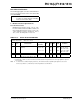
Note: This document summarizes all silicon
errata issues from all revisions of silicon,
previous as well as current. Only the
issues indicated by the shaded column in
the following tables apply to the current
silicon revision (A2).
A1 A2
X
A1 A2
X
A1 A2
X
A1 A2
X X
A1 A2
X